MCU decryption cost is set by five technical variables, not a fixed price list: the protection mechanism inside the part, the chip family and process node, whether extraction can stay non-invasive, the memory volume to read, and the turnaround you request. Roughly, an unprotected serial EEPROM read sits in the low hundreds of dollars, a lock-bit 8-bit MCU in the few-hundred range, and a hardened 32-bit part with encrypted boot flash in the thousands.
ロックビットが解除されている状態であれば一般的な処理で対応できますが、暗号化されたFlashを使用した多層セキュアブート(Secure Boot)環境は同じようには扱えません。コストはチップサイズではなく、突破または解析する必要がある保護障壁の複雑さによって決まります。詳細については MCU読み出し保護(MCU Readout Protection) を参照してください。
チップファミリとプロセスノード(Chip Family and Process Node)。
比較的大きなプロセス世代(おおよそ350 nm以上)は、130 nm未満の先端プロセスデバイスよりも解析が容易な傾向があります。STM32F1、PIC16/18、ATmegaなど、技術情報が公開されているデバイスファミリには確立された解析手法があります。一方、仕様や構造が公開されていないカスタムASICには、利用可能な標準的手法が存在しません。
侵襲的解析と非侵襲的解析(Invasive vs Non-Invasive)。
デバッグポートやブートローダーを利用したデータ取得では通常1個のサンプルで対応できます。一方、ICデキャップ(IC Decapsulation)やマイクロプロービング(Micro-Probing)を必要とする解析では、一部のチップが解析過程で消費されるため、一般的に2~5個程度のサンプルが必要になります。
データ量(Data Volume)。
8ビットデバイスから4 KBのデータを読み出す処理は、バンク構成された32ビットFlashから512 KBを取得する処理より高速に完了します。
That spread usually decides the project. An OEM that has lost its source code, a repair house keeping a discontinued line alive, a team running an authorised security review — all face one trade-off: recover the firmware, or fund a redesign. Knowing what moves the price stops you overpaying, and stops you trusting a technically impossible quote.
The Five Cost Drivers
- Protection mechanism. A cleared lock bit is routine; multi-layer secure boot with encrypted flash is not. Cost tracks the barriers to cross, not the chip’s size. See MCU readout protection.
- Chip family and process node. Coarser geometries (roughly 350 nm and up) are more tractable than sub-130 nm parts. Documented families like STM32F1, PIC16/18 and ATmega have established methods; an undocumented custom ASIC has none.
- Invasive versus non-invasive. Extraction through the debug port or bootloader needs one sample; IC decapsulation and micro-probing typically need two to five, because some are consumed.
- Data volume. Reading 4 KB from an 8-bit part is faster than 512 KB of banked 32-bit flash.
- Turnaround. Standard work runs at normal rates; a rush slot on a validated target carries a surcharge.
잠금 비트(lock bit)가 해제된 상태라면 일반적인 작업으로 처리할 수 있지만, 암호화된 Flash를 사용하는 다중 계층 보안 부트(Secure Boot) 구조는 그렇지 않습니다. 비용은 칩의 크기가 아니라 극복해야 하는 보호 장벽의 수준과 복잡성에 따라 결정됩니다. 자세한 내용은 MCU 읽기 보호(MCU Readout Protection) 를 참조하십시오.
칩 패밀리 및 공정 노드(Chip Family and Process Node).
상대적으로 미세하지 않은 공정(대략 350 nm 이상)은 130 nm 이하의 최신 공정 부품보다 분석 및 접근이 용이한 경우가 많습니다. STM32F1, PIC16/18, ATmega와 같이 문서화된 칩 패밀리는 검증된 분석 방법이 존재하지만, 문서화되지 않은 커스텀 ASIC은 활용 가능한 표준 방법이 없습니다.
침습적 방식과 비침습적 방식(Invasive vs Non-Invasive).
디버그 포트 또는 부트로더를 통한 데이터 추출은 일반적으로 하나의 샘플만 필요합니다. 반면 IC 디캡슐레이션(IC Decapsulation)과 마이크로 프로빙(Micro-Probing)을 사용하는 분석은 일부 칩이 과정 중 소모될 수 있기 때문에 일반적으로 2~5개의 샘플이 필요합니다.
데이터 용량(Data Volume).
8비트 디바이스에서 4 KB 데이터를 읽는 작업은 뱅크 구조를 가진 32비트 Flash에서 512 KB 데이터를 읽는 것보다 빠르게 처리됩니다.
Indicative Price Bands
Single part, binary delivered, market-indicative ranges:
| Part class | Indicative price (USD) | Turnaround |
|---|---|---|
| Serial EEPROM (24Cxx, 93Cxx) | $100–$300 | 1–3 days |
| 8-bit MCU (PIC16/18, ATmega) | $200–$600 | 3–7 days |
| 32-bit Cortex-M (STM32F1/F4) | $400–$1,200 | 5–10 days |
| 32-bit, enhanced protection | $800–$3,000 | 7–15 days |
| Encrypted flash, secure boot | $3,000+ | 15–40 days |
Một bit khóa (lock bit) được xóa là trường hợp xử lý thông thường; trong khi đó, hệ thống Secure Boot nhiều lớp kết hợp với Flash được mã hóa lại là một vấn đề hoàn toàn khác. Chi phí phụ thuộc vào mức độ phức tạp của các lớp bảo vệ cần vượt qua, không phụ thuộc vào kích thước của chip. Xem thêm bảo vệ đọc MCU (MCU Readout Protection).
Dòng chip và công nghệ quy trình (Chip Family and Process Node).
Các công nghệ quy trình lớn hơn (khoảng từ 350 nm trở lên) thường dễ tiếp cận và phân tích hơn so với các linh kiện sử dụng công nghệ dưới 130 nm. Những dòng chip đã được tài liệu hóa như STM32F1, PIC16/18 và ATmega có các phương pháp phân tích đã được thiết lập; trong khi một ASIC tùy chỉnh không có tài liệu công khai thường không có phương pháp tiêu chuẩn để xử lý.
Phân tích xâm nhập và không xâm nhập (Invasive vs Non-Invasive).
Việc trích xuất thông qua cổng debug hoặc bootloader thường chỉ cần một mẫu chip. Ngược lại, IC decapsulation và kỹ thuật micro-probing thường cần từ hai đến năm mẫu, vì một số chip có thể bị tiêu hao trong quá trình phân tích.
Dung lượng dữ liệu (Data Volume).
Việc đọc 4 KB dữ liệu từ một thiết bị 8-bit sẽ nhanh hơn so với việc đọc 512 KB Flash 32-bit có cấu trúc phân vùng bank.
What a Proper Quote Should Include
A serious quote names the deliverable, not just a number:
- The extracted binary as
.binor.hex - A verification note with CRC/checksum and read address range
- The protection mechanism found and the method used
- Fuse, option-byte and read-protection state recovered
- A confidence level stated before work begins
- A feasibility verdict, including “not feasible” when that is honest
How to Lower the Cost
Send the whole board rather than the bare chip where you can: it supplies the clock and boot environment the protection routine expects. Supply two or three spare samples, give the exact part number with lot and date codes, and accept standard turnaround. Each step reduces risk, and risk is what a premium covers.
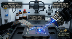
یک بیت قفل (Lock Bit) که پاک شده باشد، معمولاً یک وضعیت عادی و قابل مدیریت است؛ اما Secure Boot چندلایه همراه با Flash رمزگذاریشده شرایط کاملاً متفاوتی دارد. هزینه به اندازه فیزیکی تراشه وابسته نیست، بلکه به تعداد و پیچیدگی موانع امنیتی که باید بررسی یا عبور داده شوند بستگی دارد. برای اطلاعات بیشتر به محافظت خواندن MCU (MCU Readout Protection) مراجعه کنید.
خانواده تراشه و نود فرآیندی (Chip Family and Process Node).
فناوریهای ساخت با ابعاد بزرگتر (تقریباً 350 نانومتر و بالاتر) معمولاً نسبت به قطعات با فناوری کمتر از 130 نانومتر، دسترسی و تحلیل آسانتری دارند. خانوادههای دارای مستندات مانند STM32F1، PIC16/18 و ATmega دارای روشهای تحلیلی شناختهشده هستند؛ در حالی که یک ASIC سفارشی بدون مستندات، روش استاندارد مشخصی برای تحلیل ندارد.
تحلیل تهاجمی و غیرتهاجمی (Invasive vs Non-Invasive).
استخراج اطلاعات از طریق پورت Debug یا Bootloader معمولاً به یک نمونه تراشه نیاز دارد. اما روشهایی مانند IC Decapsulation و Micro-Probing معمولاً به دو تا پنج نمونه نیاز دارند، زیرا برخی تراشهها در فرآیند تحلیل مصرف میشوند.
حجم داده (Data Volume).
خواندن 4 کیلوبایت داده از یک قطعه 8 بیتی سریعتر از خواندن 512 کیلوبایت Flash سیودوبیتی با ساختار بانکی انجام میشود.
FAQ
Why do two vendors quote different prices for the same chip?
One has usually assessed the die revision and the other has not. A low figure on a hardened part often means the protection tier was never checked.
Is a “no fix, no fee” offer worth trusting?
It is fair on routine, documented parts. On high-security devices real feasibility is low, so it is more a sales signal than an engineering statement.
Does a higher price guarantee success?
No. Cost reflects effort and risk, not certainty. RDP Level 2, PUF-keyed storage and smartcard-grade ICs have no practical recovery path, and a credible lab says so.
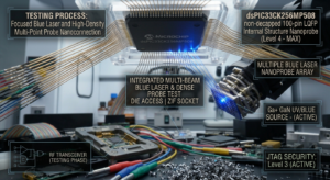
إن إزالة تفعيل بت القفل (Lock Bit) تُعد حالة اعتيادية يمكن التعامل معها، بينما لا ينطبق الأمر نفسه على نظام Secure Boot متعدد الطبقات مع ذاكرة Flash مشفرة. ترتبط التكلفة بمستوى الحواجز الأمنية التي يجب تجاوزها أو تحليلها، وليس بحجم الشريحة. راجع حماية قراءة MCU (MCU Readout Protection).
عائلة الشريحة وعقدة التصنيع (Chip Family and Process Node).
تكون التقنيات ذات الأبعاد الأكبر (تقريبًا 350 نانومتر وما فوق) أكثر قابلية للتحليل مقارنةً بالشرائح المصنعة بتقنيات أقل من 130 نانومتر. تمتلك العائلات الموثقة مثل STM32F1 وPIC16/18 وATmega طرق تحليل معروفة ومثبتة، بينما لا يمتلك ASIC مخصص وغير موثق أي طرق قياسية متاحة.
التحليل التدخلي وغير التدخلي (Invasive vs Non-Invasive).
عادةً ما يتطلب الاستخراج عبر منفذ Debug أو Bootloader عينة واحدة فقط. أما عمليات IC Decapsulation وMicro-Probing فتحتاج غالبًا إلى عينتين إلى خمس عينات، لأن بعض الشرائح يتم استهلاكها أثناء عملية التحليل.
حجم البيانات (Data Volume).
تستغرق قراءة 4 KB من جهاز 8-bit وقتًا أقل من قراءة 512 KB من ذاكرة Flash 32-bit ذات بنية مصرفية (Banked Architecture).
Getting a Realistic Figure
Send the chip marking, package and a board photo, and say what you need the binary for. We will confirm the protection mechanism, the realistic method and the cost band before any budget is committed — request a free assessment, under NDA and only on hardware you own or are authorised in writing to analyse.
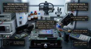
**Chip family and process node.** Coarser geometries (roughly 350 nm and up) are more tractable than sub-130 nm parts. Documented families like STM32F1, PIC16/18 and ATmega have established methods; an undocumented custom ASIC has none.
**Invasive versus non-invasive.** Extraction through the debug port or bootloader needs one sample; IC decapsulation and micro-probing typically need two to five, because some are consumed.
**Data volume.** Reading 4 KB from an 8-bit part is faster than 512 KB of banked 32-bit flash.