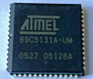
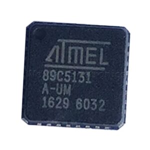
Copy MCU AT89C5131A Software from its encrypted microcontroller flash memory, the original microprocessor at89c5131a fuse bit can be unlocked and readout firmware heximal file;

Introduction
The AT89C5130A/31A-M clock controller is based on an on-chip oscillator feeding an on-chip Phase Lock Loop (PLL). All the internal clocks to the peripherals and CPU core are generated by this controller.
The AT89C5130A/31A-M X1 and X2 pins are the input and the output of a single-stage on-chip inverter (see Figure 5-1) that can be configured with off-chip components as a Pierce oscillator (see Figure 5-2). Value of capacitors and crystal characteristics are detailed in the section “DC Characteristics” if extracting at89c4051 MCU memory file.
The X1 pin can also be used as input for an external 48 MHz clock. The clock controller outputs three different clocks as shown in Figure 5-1:
- a clock for the CPU core
- a clock for the peripherals which is used to generate the Timers, PCA, WD, and Port sampling clocks
- a clock for the USB controller
These clocks are enabled or disabled depending on the power reduction mode as detailed in Section “Power Management”, page 155.
The AT89C5130A/31A-M PLL is used to generate internal high frequency clock (the USB Clock) synchronized with an external low-frequency (the Peripheral Clock). The PLL clock is used to generate the USB interface clock. Figure 5-3 shows the internal structure of the PLL.
The PFLD block is the Phase Frequency Comparator and Lock Detector. This block makes the comparison between the reference clock coming from the N divider and the reverse clock coming from the R divider and generates some pulses on the Up or Down signal depending on the edge position of the reverse clock. The PLLEN bit in PLLCON register is used to enable the clock generation. When the PLL is locked, the bit PLOCK in PLLCON register is set.
The CHP block is the Charge Pump that generates the voltage reference for the VCO by injecting or extracting charges from the external filter connected on PLLF pin (see Figure 5-4). Value of the filter components are detailed in the Section “DC Characteristics”.

The VCO block is the Voltage Controlled Oscillator controlled by the voltage VREF produced by the charge pump. It generates a square wave signal: the PLL clock.
The Special Function Registers (SFRs) of the AT89C5130A/31A-M fall into the following categories:
- C51 core registers: ACC, B, DPH, DPL, PSW, SP
- I/O port registers: P0, P1, P2, P3, P4
- Timer registers: T2CON, T2MOD, TCON, TH0, TH1, TH2, TMOD, TL0, TL1, TL2, RCAP2L, RCAP2H
- Serial I/O port registers: SADDR, SADEN, SBUF, SCON when extract at89s53 MCu code
- PCA (Programmable Counter Array) registers: CCON, CMOD, CCAPMx, CL, CH, CCAPxH, CCAPxL (x: 0 to 4)
- Power and clock control registers: PCON
- Hardware Watchdog Timer registers: WDTRST, WDTPRG
- Interrupt system registers: IEN0, IPL0, IPH0, IEN1, IPL1, IPH1
- Keyboard Interface registers: KBE, KBF, KBLS
- LED register: LEDCON
- Two Wire Interface (TWI) registers: SSCON, SSCS, SSDAT, SSADR
- Serial Port Interface (SPI) registers: SPCON, SPSTA, SPDAT
- USB registers: Uxxx (17 registers)
- PLL registers: PLLCON, PLLDIV before Copy MCU
- BRG (Baud Rate Generator) registers: BRL, BDRCON
- Flash register: FCON (FCON access is reserved for the Flash API and ISP software)
- EEPROM register: EECON
- Others: AUXR, AUXR1, CKCON0, CKCON1The AT89C5130A/31A-M implement 16/ 32 Kbytes of on-chip program/code memory. Figure 8-1 shows the split of internal and external program/code memory spaces depending on the product.The Flash memory increases EPROM and ROM functionality by in-circuit electrical erasure and programming.
- Thanks to the internal charge pump, the high voltage needed for programming or erasing Flash cells is generated on-chip using the standard VDD voltage. Thus, the Flash Memory can be programmed using only one voltage and allows In- application Software Programming commonly known as IAP. Hardware programming mode is also available using specific programming tool.

