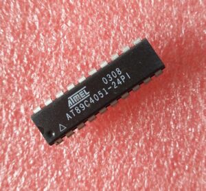
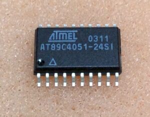
Extract IC AT89C4051 Code out from the flash and eeprom memory, the status of Microcontroller AT89C4051 will be reset to opened one after crack MCU security fuse bit;
The AT89C4051 is a low-voltage, high-performance CMOS 8-bit microcontroller with 4K bytes of Flash programmable and erasable read-only memory. The device is manufactured using Atmel’s high-density nonvolatile memory technology and is compatible with the industry-standard MCS-51 instruction set.
By combining a versatile 8-bit CPU with Flash on a monolithic chip, the Atmel AT89C4051 is a powerful microcontroller which provides a highly-flexible and cost-effective solution to many embedded control applications. The AT89C4051 provides the following standard features: 4K bytes of Flash, 128 bytes of RAM, 15 I/O lines, two 16-bit timer/counters, a five-vector, two-level interrupt architecture, a full duplex serial port, a precision analog comparator, on-chip oscillator and clock circuitry if Extract mcu at89lv51 binary.
In addition, the AT89C4051 is designed with static logic for operation down to zero frequency and supports two software-selectable power saving modes. The Idle Mode stops the CPU while allowing the RAM, timer/counters, serial port and interrupt system to continue functioning. The power-down mode saves the RAM contents but freezes the oscillator disabling all other chip functions until the next hardware reset.
Port 1 is an 8-bit bi-directional I/O port. Port pins P1.2 to P1.7 provide internal pullups. P1.0 and P1.1 require external pullups. P1.0 and P1.1 also serve as the positive input (AIN0) and the negative input (AIN1), respectively, of the on-chip precision analog comparator. The Port 1 output buffers can sink 20 mA and can drive LED displays directly. When 1s are written to Port 1 pins, they can be used as inputs. When pins P1.2 to P1.7 are used as inputs and are externally pulled low, they will source cur

rent (IIL) because of the internal pullups.
Port 1 also receives code data during Flash programming and verification. Port 3 pins P3.0 to P3.5, P3.7 are seven bi-directional I/O pins with internal pullups. P3.6 is hard-wired as an input to the output of the on-chip comparator and is not accessible as a general-purpose I/O pin. The Port 3 output buffers can sink 20 mA. When 1s are written to Port 3 pins they are pulled high by the internal pullups and can be used as inputs. As inputs, Port 3 pins that are externally being pulled low will source current (IIL) because of the pullups.
Port 3 also serves the functions of various special features of the AT89C4051 as listed below: Port 3 also receives some control signals for Flash programming and verification.
XTAL1 and XTAL2 are the input and output, respectively, of an inverting amplifier which can be configured for use as an on-chip oscillator, as shown in Figure 5-1. Either a quartz crystal or ceramic resonator may be used. To drive the device from an external clock source, XTAL2 should be left unconnected while XTAL1 is driven as shown in Figure 5-2. There are no requirements on the duty cycle of the external clock signal, since the input to the internal clocking circuitry is through a divide-by-two flip-flop, but minimum and maximum voltage high and low time specifications must be observed if Extract microcontroller at89c1051 code.
The AT89C4051 is an economical and cost-effective member of Atmel’s growing family of microcontrollers. It contains 4K bytes of Flash program memory. It is fully compatible with the MCS-51 architecture, and can be programmed using the MCS-51 instruction set. However, there are a few considerations one must keep in mind when utilizing certain instructions to program this device.
All the instructions related to jumping or branching should be restricted such that the destination address falls within the physical program memory space of the device, which is 4K for the AT89C4051. This should be the responsibility of the software programmer. For example, LJMP 0FE0H would be a valid instruction for the AT89C4051 (with 4K of memory), whereas LJMP 1000H would not.