Extract Microcontroller AT89S53 Code from its flash and eeprom memory, crack MCU process will help engineer to disable the security fuse bit inside the AT89S53 and its tamper resistance system;
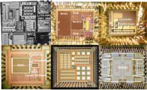
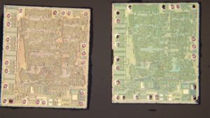
Extracting microcontroller AT89S53 code is a sophisticated process that combines knowledge of embedded systems, hardware hacking, and security exploitation. The AT89S53, developed by Atmel, is a powerful 8-bit microcontroller featuring 12K bytes of in-system programmable Flash memory, 256 bytes of RAM, and 32 I/O lines. It supports ISP (In-System Programming) and SPI (Serial Peripheral Interface) for programming and data transfer. However, once its memory is locked and secured, it becomes extremely difficult to access or recover the original firmware or source code.
Port 2 is an 8-bit bidirectional I/O port with internal pullups. The Port 2 output buffers can sink/source four TTL inputs. When 1s are written to Port 2 pins, they are pulled high by the internal pullups and can be used as inputs. As inputs, Port 2 pins that are externally being pulled low will source current (IIL) because of the internal pullups.
Port 2 emits the high-order address byte during fetches from external program memory and during accesses to external data memory that use 16-bit addresses (MOVX @ DPTR). In this application, Port 2 uses strong internal pullups when emitting 1s. During accesses to external data memory that use 8-bit addresses (MOVX @ RI), Port 2 emits the contents of the P2 Special Function Register.
Port 2 also receives the high-order address bits and some control signals during Flash programming and verification. Port 3 is an 8 bit bidirectional I/O port with internal pullups. The Port 3 output buffers can sink/source four TTL inputs. When 1s are written to Port 3 pins, they are pulled high by the internal pullups and can be used as inputs. As inputs, Address Latch Enable is an output pulse for latching the low byte of the address during accesses to external memory after Extract Microcontroller embedded firmware.
This pin is also the program pulse input (PROG) during Flash programming. In normal operation, ALE is emitted at a constant rate of 1/6 the oscillator frequency and may be used for external timing or clocking purposes. Note, however, that one ALE pulse is skipped during each access to external data memory before read Microcontroller firmware.
If desired, ALE operation can be disabled by setting bit 0 of SFR location 8EH. With the bit set, ALE is active only during a MOVX or MOVC instruction. Otherwise, the pin is weakly pulled high. Setting the ALE-disable bit has no effect if the microcontroller is in external execution mode.
The AT89S53 implements 256 bytes of RAM. The upper 128 bytes of RAM occupy a parallel space to the Special Function Registers. That means the upper 128 bytes have the same addresses as the SFR space but are physically separate from SFR space.
When an instruction accesses an internal location above address 7FH, the address mode used in the instruction specifies whether the CPU accesses the upper 128 bytes of RAM or the SFR space. Instructions that use direct addressing access SFR space.
For example, the following direct addressing instruction accesses the SFR at location 0A0H (which is P2). MOV 0A0H, #data Instructions that use indirect addressing access the upper 128 bytes of RAM. For example, the following indirect addressing instruction, where R0 contains 0A0H, accesses the data byte at address 0A0H, rather than P2 (whose address is 0A0H).
MOV @R0, #data Note that stack operations are examples of indirect addressing, so the upper 128 bytes of data RAM are available as stack space. The programmable Watchdog Timer (WDT) operates from an independent oscillator. The prescaler bits, PS0, PS1 and PS2 in SFR WCON are used to set the period of the Watchdog Timer from 16 ms to 2048 ms. The available timer periods are shown in the following table and the actual timer periods (at VCC = 5V) are within ±30% of the nominal.
The WDT is disabled by Power-on Reset and during Power-down. It is enabled by setting the WDTEN bit in SFR WCON (address = 96H). The WDT is reset by setting the WDTRST bit in WCON. When the WDT times out without being reset or disabled, an internal RST pulse is generated to reset the CPU.