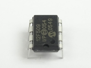
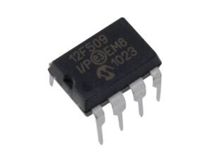
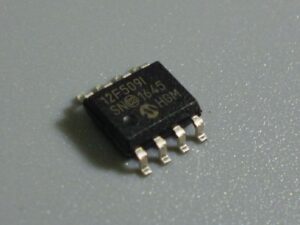
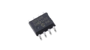
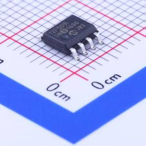
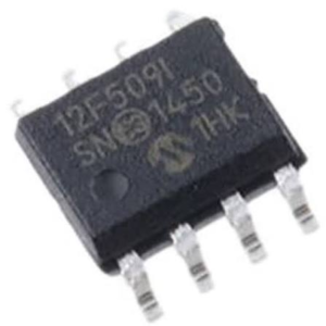
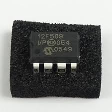
The PIC12F509 microcontroller is a compact yet highly efficient 8-bit MCU designed for embedded systems that demand low cost, stability, and minimal hardware footprint. Featuring an internal oscillator, OTP program memory, and a streamlined instruction set, this chip is widely deployed in consumer electronics, power management modules, remote controllers, security devices, and small industrial automation systems. Despite its simplicity, the PIC12F509 often carries critical firmware and control logic stored within its internal memory. To protect intellectual property, manufacturers frequently configure the chip as secured, protected, encrypted, or locked, restricting direct access to the program, source code, and embedded data. This makes it difficult to open or retrieve the binary or heximal file from the microcontroller under normal conditions.
After generating a START condition, the bus master transmits a control byte consisting of a slave address and a Read/Write bit that indicates what type of operation is to be performed.
The slave address consists of a 4-bit device code (1010) followed by three don’t care bits. The last bit of the control byte determines the operation to be performed. When set to a one a read operation is selected, and when set to a zero a write operation is selected. (Figure 7-5). The bus is monitored for its corresponding slave address all the time. It generates an acknowledge bit if the slave address was true and it is not in a programming mode. Following the start signal from the master, the device code (4 bits), the don’t care bits (3 bits), and the R/W bit (which is a logic low) are placed onto the bus by the master transmitter. This indicates to the addressed slave receiver that a byte with a word address will follow after it has generated an acknowledge bit during the ninth clock cycle. Therefore, the next byte transmitted by the master is the word address and will be written into the address pointer.
Only the lower four address bits are used by the device, and the upper four bits are don’t cares. The address byte is acknowledgeable and the master device will then transmit the data word to be written into the addressed memory location. The memory acknowledges again and the master generates a stop condition. This initiates the internal write cycle, and during this time will not generate acknowledge signals (Figure 7-7). After a byte write command, the internal address counter will not be incremented and will point to the same address location that was just written. If a stop bit is transmitted to the device at any point in the write command sequence before the entire sequence is complete, then the command will abort and no data will be written.
If more than 8 data bits are transmitted before the stop bit is sent, then the device will clear the previously loaded byte and begin loading the data buffer again. If more than one data byte is transmitted to the device and a stop bit is sent before a full eight data bits have been transmitted, then the write command will abort and no data will be written. The EEPROM memory employs a VCC threshold detector circuit which disables the internal erase/write logic if the VCC is below minimum VDD. Byte write operations must be preceded and immediately followed by a bus not busy bus cycle where both SDA and SCL are held high.
In many real-world cases, engineers need to hack, extract, recover, restore, or reverse engineering a PIC12F509 when original firmware, source code, or archive documentation is no longer available. The microcontroller may hold essential program instructions, yet its locked configuration prevents direct reading of memory, flash, or EEPROM. Extracting a binary dump or reconstructing a heximal file requires specialized handling of the MCU to safely access its internal data structures. The process involves recovering firmware, program files, and memory archives while maintaining data integrity. Without proper extraction, critical system functions embedded in the chip could be permanently inaccessible, leading to operational downtime or costly redesign efforts.
Technically, the process to extract IC PIC12F509 heximal data from a secured, protected, encrypted, or locked chip involves overcoming multiple embedded security mechanisms. To hack, extract, recover, open, restore, or reverse engineering the MCU, specialists must deal with read-protection bits that prevent access to firmware, source code, binary, heximal program, and memory file systems. The chip’s internal architecture may restrict direct dumping of EEPROM or flash data, requiring advanced approaches to retrieve a complete archive. Ensuring the accuracy of the dump is critical, as any corruption in firmware, data, or program structure can affect usability. Engineers must carefully manage the extraction process to preserve the integrity of the microcontroller’s memory, allowing for successful reconstruction of the original program and archive files.
Successfully recovering and restoring data from a PIC12F509 microcontroller provides significant value for clients working with legacy or unsupported systems. By extracting firmware, binary files, and source code archives, businesses can duplicate or replicate the original MCU functionality, enabling maintenance, repair, and continued production. Reverse engineering also allows detailed analysis of the program and memory data, supporting optimization or migration to modern microprocessor or microcontroller platforms. For industries relying on long-term equipment operation, this capability reduces replacement costs and extends product lifecycle. Ultimately, extracting heximal and binary data from a secured MCU transforms restricted information into a practical resource, empowering clients to regain control over their embedded systems and ensure long-term operational stability.