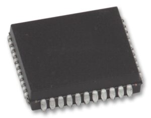
The demand to read MCU AT89C51ID2 file arises in various sectors—from embedded legacy system restoration to competitive analysis and hardware security audits. The AT89C51ID2, a powerful 8-bit microcontroller from Microchip (formerly Atmel), features in-system programmable Flash memory, high-speed UART, SPI, and a watchdog timer. What makes this chip stand out is its secured architecture, which includes features like protected Flash memory and encrypted program storage, often configured with lock bits to prevent unauthorized access.
Extracting a binary or heximal file from a secured AT89C51ID2 is not a trivial task. The process typically requires specialized hardware and sophisticated techniques to crack, break, or attack the chip’s security layers. One of the key challenges lies in the microcontroller’s ability to disable external memory read operations once its lock bits are set, effectively making its firmware and data inaccessible through conventional means.
To recover, replicate, or duplicate the program stored inside such a protected MCU, advanced methods such as decapsulation, voltage glitching, or optical fault injection are often applied. These hardware-level techniques expose the chip die for analysis or cause it to enter unintended states, allowing for a dump of its internal flash, EEPROM, or memory segments.
Security-focused reverse engineers also resort to reverse engineering the MCU’s logic by observing its behavior under controlled stimuli, ultimately enabling them to decode or decrypt the stored source code or binary archive. Once successfully copied or cloned, this data can then be restored to a fresh AT89C51ID2 or a compatible microcontroller, enabling program duplication or firmware recovery for system continuity.
Read MCU AT89C51ID2 File from its memory which include flash and eeprom, the status of Microcontroller will be reset to unlocked after Crack MCU security fuse bits;
Each module in the PCA has a special function register associated with it. These registers are: CCAPM0 for module 0, CCAPM1 for module 1, etc. (See Table 28). The registers contain the bits that control the mode that each module will operate in.
The ECCF bit (CCAPMn.0 where n=0, 1, 2, 3, or 4 depending on the module) enables the CCF flag in the CCON SFR to generate an interrupt when a match or compare occurs in the associated module.
PWM (CCAPMn.1) enables the pulse width modulation mode. The TOG bit (CCAPMn.2) when set causes the CEX output associated with the module to toggle when there is a match between the PCA counter and the module’s capture/compare register if copy MCU at89c5131a software.
The match bit MAT (CCAPMn.3) when set will cause the CCFn bit in the CCON register to be set when there is a match between the PCA counter and the module’s capture/compare register. The next two bits CAPN (CCAPMn.4) and CAPP (CCAPMn.5) determine the edge that a capture input will be active on. The CAPN bit enables the negative edge, and the CAPP bit enables the positive edge. If both bits are set both edges will be enabled and a capture will occur for either transition.
The last bit in the register ECOM (CCAPMn.6) when set enables the comparator function. There are two additional registers associated with each of the PCA modules. They are CCAPnH and CCAPnL and these are the registers that store the 16-bit count when a capture occurs or a compare should occur. When a module is used in the PWM mode these registers are used to control the duty cycle of the output (See Table 30 & Table 31) before extract microcontroller at89ls8252 code.
To use one of the PCA modules in the capture mode either one or both of the CCAPM bits CAPN and CAPP for that module must be set. The external CEX input for the module (on port 1) is sampled for a transition. When a valid transition occurs the PCA hardware loads the value of the PCA counter registers (CH and CL) into the module’s capture registers (CCAPnL and CCAPnH). If the CCFn bit for the module in the CCON SFR and the ECCFn bit in the CCAPMn SFR are set then an interrupt will be generated.
Before enabling ECOM bit, CCAPnL and CCAPnH should be set with a non zero value, otherwise an unwanted match could happen. Writing to CCAPnH will set the ECOM bit. Once ECOM set, writing CCAPnL will clear ECOM so that an unwanted match doesn’t occur while modifying the compare value. Writing to CCAPnH will set ECOM. For this reason, user software should write CCAPnL first, and then CCAPnH. Of course, the ECOM bit can still be controlled by accessing to CCAPMn register.
However, it’s important to acknowledge the legal and ethical implications of such operations. While these techniques are invaluable for restoring malfunctioning legacy systems or performing vulnerability assessments, they can also be misused for intellectual property theft or malicious tampering.
In conclusion, the ability to read MCU AT89C51ID2 file from a locked or encrypted device involves a complex set of techniques designed to attack and bypass embedded protections. Whether the goal is to restore critical legacy functionality or to analyze security resilience, this area of embedded systems research continues to evolve with both innovation and caution.
In this mode the CEX output (on port 1) associated with the PCA module will toggle each time a match occurs between the PCA counter and the module’s capture registers.
To activate this mode the TOG, MAT, and ECOM bits in the module’s CCAPMn SFR must be set.
A prior write must be done to CCAPnL and CCAPnH before writing the ECOMn bit. Before enabling ECOM bit, CCAPnL and CCAPnH should be set with a non zero value, otherwise an unwanted match could happen. Once ECOM set, writing CCAPnL will clear ECOM so that an unwanted match doesn’t occur while modifying the compare value. Writing to CCAPnH will set ECOM. For this reason, user software should write CCAPnL first, and then CCAPnH. Of course, the ECOM bit can still be controlled by accessing to CCAPMn register.