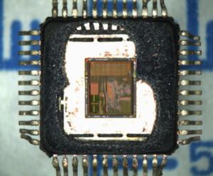
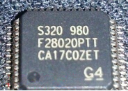
DSP Microcontroller TMS320F28020 Flash Memory Cracking will need to remove its security fuse bit by unlocking dsp tms320f28020 controller, then recover embedded flash program from mcu tms320f28020;
When the code-security passwords are programmed, all addresses between 0x3F7F80 and 0x3F7FF5 cannot be used as program code or data. These locations must be programmed to 0x0000.
If the code security feature is not used, addresses 0x3F7F80 through 0x3F7FEF may be used for code or data to extract dsp mcu tms320f28016 firmware. Addresses 0x3F7FF0 – 0x3F7FF5 are reserved for data and should not contain program code.
On ROM devices, addresses 0x3F7FF0 – 0x3F7FF5 and 0x3D7BFC – 0x3D7BFF are reserved for TI, irrespective of whether code security has been used or not. User application should not use these locations in any way. Below Table shows how to handle these memory locations.
Peripheral Frame 1 and Peripheral Frame 2 are grouped together so as to enable these blocks to be write/read peripheral block protected. The protected mode ensures that all accesses to these blocks happen as written.
Because of the C28x pipeline, a write immediately followed by a read, to different memory locations, will appear in reverse order on the memory bus of the CPU. This can cause problems in certain peripheral applications where the user expected the write to occur first (as written).
The C28x CPU supports a block protection mode where a region of memory can be protected so as to make sure that operations occur as written to execute tms320f28015 microprocessor flash memory binary reading (the penalty is extra cycles are added to align the operations). This mode is programmable and by default, it will protect the selected zones.