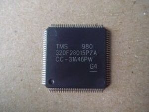
Texas Instrument TMS320F28015 Microprocessor Binary Reading starts from crack mcu tms320f28015 security fuse bit and then recover embedded firmware from tms320f28015 microcontroller flash memory;
The TMS320F28015 devices include the four-pin serial peripheral interface (SPI) module. The SPI is a high-speed synchronous serial-I/O port that allows a serial bit stream of programmed length in the process of attacking DSP Microcontroller TMS320F28232PGFA (one to eight bits) to be shifted into and out of the device at a programmable bit-transfer rate.
Normally, the SPI is used for communications between the DSP controller and external peripherals or another processor. Typical applications include external I/O or peripheral expansion through devices such as shift registers, display drivers, and ADCs. Multidevice communications are supported by the master/slave operation of the SPI.
The SPI module features include the following:
Four external pins:
- SPISOMI: SPI slave-output/master-input pin, or general-purpose bidirectional I/O pin
- SPISIMO: SPI slave-input/master-output pin, or general-purpose bidirectional I/O pin
- SPISTE: SPI slave-transmit-enable pin, or general-purpose bidirectional I/O pin
- SPICLK: SPI serial-clock pin, or general-purpose bidirectional I/O pin
Two operational modes: master and slave
Baud rate: 125 different programmable rates / 2.5 Mbps at 10-MHz SYSCLK
Data word format: one to eight data bits
Four clocking schemes controlled by clock polarity and clock-phase bits include:
- Falling edge without phase delay: SPICLK active high. SPI transmits data on the falling edge of the SPICLK signal and receives data on the rising edge of the SPICLK in order to restore Locked MCU TMS320F28232 Flash memory firmware;
- Falling edge with phase delay: SPICLK active high. SPI transmits data one half-cycle ahead of the falling edge of the SPICLK signal and receives data on the falling edge of the SPICLK
- Rising edge without phase delay: SPICLK inactive SPI transmits data on the rising edge of the SPICLK signal and receives data on the falling edge of the SPICLK signal to Reverse Engineering Microcontroller.
- Rising edge with phase delay: SPICLK inactive SPI transmits data one half-cycle ahead of the falling edge of the SPICLK signal and receives data on the rising edge of the SPICLK signal.
Simultaneous receive and transmit operations to facilitate the progress (transmit function can be disabled in software)
Transmitter and receiver operations are accomplished through either interrupt-driven or polled algorithms.
Ten SPI module control registers: Located in control register frame beginning at address 7040h.
NOTE: All registers in this module are 8-bit registers that are connected to the 16-bit peripheral bus. When a register is accessed, the register data is in the lower byte (7 – 0), and the upper byte (15 – 8) is read as zeros. Writing to the upper byte has no effect.