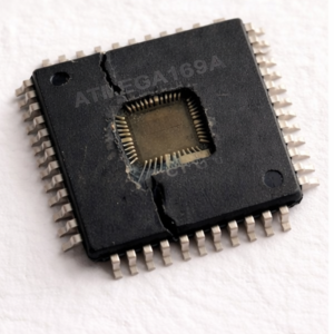
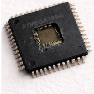
The ATmega169A microcontroller, manufactured by Microchip Technology (formerly Atmel), represents a sophisticated 8-bit AVR RISC-based processor that has been widely deployed across numerous industries. This microcontroller features 16KB of Flash memory, 512 bytes of EEPROM, and 1KB of SRAM, making it ideal for applications requiring both processing power and integrated peripheral control. The chip incorporates an on-chip LCD controller capable of driving up to 100 segments, which explains its extensive use in display-intensive applications. Engineers and system integrators frequently encounter this microprocessor in industrial control systems, medical devices, consumer electronics, and automotive applications where reliable operator interfaces are essential. The device operates at speeds up to 16MHz with supply voltages ranging from 1.8V to 5.5V, offering the flexibility required for diverse deployment scenarios.
When changing the TOP value the program must ensure that the new TOP value is higher or equal to the value of all of the Compare Registers. If the TOP value is lower than any of the Compare Registers, a compare match will never occur between the TCNTn and the OCRnx. Note that when using fixed TOP values, the unused bits are masked to zero when any of the OCRnx Registers are written.
As the third period shown in Figure 56 illustrates, changing the TOP actively while the Timer/Counter is running in the phase correct mode can result in an unsymmetrical output. The reason for this can be found in the time of update of the OCRnx Register.
Since the OCRnx update occurs at TOP, the PWM period starts and ends at TOP. This implies that the length of the falling slope is determined by the previous TOP value, while the length of the rising slope is determined by the new TOP value.
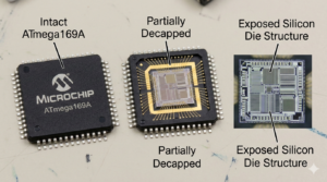
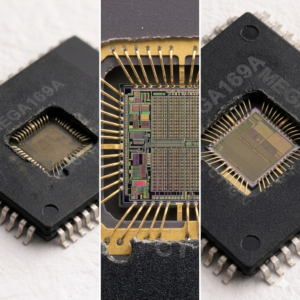
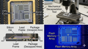
When manufacturers develop products using the ATmega169A, they typically implement secured access measures to protect their intellectual property. The microcontroller features multiple protection mechanisms including lock bits that, when programmed, prevent unauthorized reading of the internal Flash and EEPROM memory contents. These secured configurations create significant challenges when original firmware is lost due to supplier discontinuation, lack of documentation, or microcontroller failure within deployed systems. The protected state of these devices means that standard programming interfaces cannot access the binary instructions stored within. Engineers seeking to recover operational functionality must employ specialized reverse engineering techniques to extract the necessary program data from locked devices while maintaining absolute respect for intellectual property rights and applicable laws.
When these two values differ the two slopes of the period will differ in length. The difference in length gives the unsymmetrical result on the output. It is recommended to use the phase and frequency correct mode instead of the phase correct mode when changing the TOP value while the Timer/Counter is running. When using a static TOP value there are practically no differences between the two modes of operation.
In phase correct PWM mode, the compare units allow generation of PWM waveforms on the OCnx pins. Setting the COMnx1:0 bits to two will produce a non-inverted PWM and an inverted PWM output can be generated by setting the COMnx1:0 to three.
The actual OCnx value will only be visible on the port pin if the data direction for the port pin is set as output (DDR_OCnx). The PWM waveform is generated by setting (or clearing) the OCnx Register at the compare match between OCRnx and TCNTn when the counter increments, and clearing (or setting) the OCnx Register at compare match between OCRnx and TCNTn when the counter decrements.
The process to copy MCU code from a secured ATmega169A involves sophisticated technical approaches that differ fundamentally from reading an unprotected device. When facing encrypted or locked microcontrollers, our engineering team utilizes advanced reverse engineering methodologies to open access to the protected memory space. The objective is to restore the complete firmware image including the Flash program, EEPROM data, and configuration fuses that define device operation. This recovery operation produces a full binary dump containing the executable code and calibration constants necessary for proper device function. The resulting heximal format file captures every aspect of the original program, enabling complete archive and subsequent reproduction of the microcontroller‘s functionality. This extracted data represents the complete source of device behavior, though not in human-readable source code form.
The PWM frequency for the output when using phase correct PWM can be calculated by the following equation:
The N variable represents the prescaler divider (1, 8, 64, 256, or 1024). The extreme values for the OCRnx Register represent special cases when generating a PWM waveform output in the phase correct PWM mode.
If the OCRnx is set equal to BOTTOM the output will be continuously low and if set equal to TOP the output will be continuously high for non-inverted PWM mode.
For inverted PWM the output will have the opposite logic values. If OCR1A is used to define the TOP value (WGM13:0 = 11) and COM1A1:0 = 1, the OC1A output will toggle with a 50% duty cycle.
The ability to recover firmware from secured ATmega169A devices delivers substantial benefits across multiple scenarios. For manufacturers facing end-of-life challenges, extracted program images enable continued production without complete system redesign. Companies maintaining legacy equipment can restore functionality when original microcontroller fail, avoiding costly downtime. The recovered binary archive provides insurance against supply chain disruptions and supports remanufacturing efforts for products where the original source code has been lost. Whether the goal is to clone a board for production continuity, duplicate a design for fleet expansion, or simply recover data from failed components, professional reverse engineering of secured MCUs represents a critical capability for organizations dependent on embedded systems. This technical expertise ensures that valuable program intellectual property remains accessible even when original development resources are no longer available.