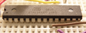
Copy Microcontroller ATmega48P Flash is a specialized technical service designed to retrieve binary or heximal firmware files from a secured or locked ATmega48P microcontroller. In many embedded products, the firmware stored inside the flash memory of the MCU contains the operational program, control algorithms, and device communication logic. When security fuse bits are enabled, the chip becomes protected and conventional programming tools cannot open or read the internal flash or EEPROM memory areas. In such situations, professional reverse engineering techniques are required to extract, recover, and restore the original firmware archive from the microprocessor. The goal is to obtain a consistent binary dump of the program memory while preserving the structure of the stored data and avoiding corruption of the secured MCU.
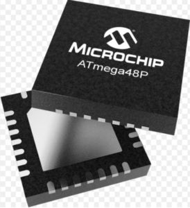
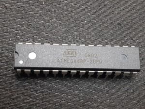
The ATmega48P microcontroller is based on the AVR 8-bit RISC architecture and is designed for reliable performance in compact embedded systems. It integrates flash program memory, EEPROM for non-volatile data storage, and SRAM for runtime operations. In addition, the chip includes SPI, USART, and TWI communication interfaces, multiple timers with PWM outputs, analog-to-digital conversion modules, watchdog timers, and configurable GPIO pins. Because of its efficiency and flexible peripheral set, the ATmega48P chip is widely deployed in industrial control modules, sensor monitoring systems, consumer electronics, home automation devices, security controllers, and energy management equipment. In these applications, the MCU acts as the core microprocessor executing firmware instructions stored in flash memory while managing real-time signals and external device communication.
The Timer/Counter can be clocked by an internal or an external clock source. The clock source is selected by the Clock Select logic which is controlled by the Clock Select (CSn2:0) bits located in the Timer/Counter control Register B (TCCRnB). For details on clock sources and prescaler, see “Timer/Counter0, Timer/Counter1, Timer/Counter3, Timer/Counter4, and Timer/Counter5 Prescalers” on page 169.
The main part of the 16-bit Timer/Counter is the programmable 16-bit bi-directional counter unit. Figure 50 shows a block diagram of the counter and its surroundings.
The 16-bit counter is mapped into two 8-bit I/O memory locations: Counter High (TCNTnH) containing the upper eight bits of the counter, and Counter Low (TCNTnL) containing the lower eight bits. The TCNTnH Register can only be indirectly accessed by the CPU. When the CPU does an access to the TCNTnH I/O location, the CPU accesses the high byte temporary register (TEMP). The temporary register is updated with the TCNTnH value when the TCNTnL is read, and TCNTnH is updated with the temporary register value when TCNTnL is written.
This allows the CPU to read or write the entire 16-bit counter value within one clock cycle via the 8-bit data bus. It is important to notice that there are special cases of writing to the TCNTn Register when the counter is counting that will give unpredictable results. The special cases are described in the sections where they are of importance.
Depending on the mode of operation used, the counter is cleared, incremented, or decremented at each timer clock (clkTn). The clkTn can be generated from an external or internal clock source, selected by the Clock Select bits (CSn2:0). When no clock source is selected (CSn2:0 = 0) the timer is stopped. However, the TCNTn value can be accessed by the CPU, independent of whether clkTn is present or not. A CPU write overrides (has priority over) all counter clear or count operations.
The counting sequence is determined by the setting of the Waveform Generation mode bits (WGMn3:0) located in the Timer/Counter Control Registers A and B (TCCRnA and TCCRnB). There are close connections between how the counter behaves (counts) and how waveforms are generated on the Output Compare outputs OCnx. For more details about advanced counting sequences and waveform generation, see “Modes of Operation” on page 147.
The Timer/Counter Overflow Flag (TOVn) is set according to the mode of operation selected by the WGMn3:0 bits. TOVn can be used for generating a CPU interrupt.
The Timer/Counter incorporates an input capture unit that can capture external events and give them a time-stamp indicating time of occurrence. The external signal indicating an event, or multiple events, can be applied via the ICPn pin or alternatively, for the Timer/Counter1 only, via the Analog Comparator unit. The time-stamps can then be used to calculate frequency, duty-cycle, and other features of the signal applied. Alternatively the time-stamps can be used for creating a log of the events.
Copy Microcontroller ATmega48P Flash projects often require engineers to hack access to a secured or encrypted MCU in order to extract, recover, and restore firmware data from protected flash and EEPROM memory. A locked chip typically blocks attempts to open its program memory through read-protection fuse settings. When engineers attempt to dump the firmware, the microcontroller may prevent access or trigger memory erase procedures designed to protect the stored source code and binary archive. Reverse engineering a protected ATmega48P therefore requires careful analysis of the chip architecture and its security configuration. The objective is to extract a stable binary or heximal file from flash program space and EEPROM data regions while preserving encrypted segments and maintaining the integrity of the recovered firmware archive. The process must be controlled to avoid damaging the MCU or corrupting critical program data during the extraction phase.
Successfully recovering firmware from a protected ATmega48P microcontroller offers important benefits for product developers and manufacturers. By restoring the firmware archive and generating a verified binary dump, clients can resume halted production lines, repair legacy electronic devices, and migrate embedded software to newer microcontroller platforms. Access to the recovered program memory also allows engineers to analyze firmware behavior, verify system functions, and recreate missing source code when original development files are unavailable. Instead of redesigning an entire electronic system, companies can rely on recovered firmware data to maintain product compatibility and extend the operational life of their equipment. Ultimately, Copy Microcontroller ATmega48P Flash services transform a locked and inaccessible MCU into a recoverable technical asset, protecting intellectual property and preserving the embedded knowledge stored within secured microcontroller memory.