The demand to read microcontroller ATmega640 software is growing as embedded systems based on this high-capacity AVR platform continue to operate in long-life products. The ATmega640 is a powerful 8-bit microcontroller (MCU) featuring up to 64 KB of flash program memory, integrated EEPROM, ample SRAM, multiple UARTs, SPI, I²C, advanced timers, and rich interrupt handling. These capabilities make the chip a preferred choice for complex control logic in industrial automation, communication equipment, instrumentation, medical devices, and professional-grade consumer electronics.
In many deployed systems, the complete firmware or original source code is no longer available. When this happens, engineers must extract the embedded binary or heximal program directly from the ATmega640 chip. The goal is to recover critical operational data, configuration parameters, and control algorithms stored across memory regions such as flash and EEPROM, then organize them into a structured archive or readable file for analysis and reuse.
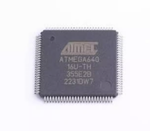
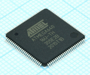
Read Microcontroller ATmega640 Software needs to reverse engineering microcontroller atmega640 structure and then extract embedded heximal from MCU’s flash and eeprom memory
Features
- High Performance, Low Power AVR® 8-Bit Microcontroller
- Advanced RISC Architecture
– 135 Powerful Instructions – Most Single Clock Cycle Execution
– 32 x 8 General Purpose Working Registers
– Fully Static Operation
– Up to 16 MIPS Throughput at 16 MHz
– On-Chip 2-cycle Multiplier
High Endurance Non-volatile Memory Segments
– 64K/128K/256K Bytes of In-System Self-Programmable Flash
– 4K Bytes EEPROM
– 8K Bytes Internal SRAM before Read Microcontroller
– Write/Erase Cycles:10,000 Flash/100,000 EEPROM
– Data retention: 20 years at 85°C/ 100 years at 25°C
– Optional Boot Code Section with Independent Lock Bits
- In-System Programming by On-chip Boot Program
- True Read-While-Write Operation
– Programming Lock for Software Security
Endurance: Up to 64K Bytes Optional External Memory Space
JTAG (IEEE std. 1149.1 compliant) Interface
– Boundary-scan Capabilities According to the JTAG Standard
– Extensive On-chip Debug Support
– Programming of Flash, EEPROM, Fuses, and Lock Bits through the JTAG Interface
Peripheral Features if Read Microcontroller
– Two 8-bit Timer/Counters with Separate Prescaler and Compare Mode
– Four 16-bit Timer/Counter with Separate Prescaler, Compare- and Capture Mode
– Real Time Counter with Separate Oscillator
– Four 8-bit PWM Channels before Read Microcontroller
– Six/Twelve PWM Channels with Programmable Resolution from 2 to 16 Bits
(ATmega1281/2561, ATmega640/1280/2560)
– Output Compare Modulator
– 8/16-channel, 10-bit ADC (ATmega1281/2561, ATmega640/1280/2560)
– Two/Four Programmable Serial USART (ATmega1281/2561,ATmega640/1280/2560)
– Master/Slave SPI Serial Interface
– Byte Oriented 2-wire Serial Interface
– Programmable Watchdog Timer with Separate On-chip Oscillator
– On-chip Analog Comparator
– Interrupt and Wake-up on Pin Change
Special Microcontroller Features
– Power-on Reset and Programmable Brown-out Detection
– Internal Calibrated Oscillator
– External and Internal Interrupt Sources
– Six Sleep Modes: Idle, ADC Noise Reduction, Power-save, Power-down, Standby, and Extended Standby I/O and Packages
– 54/86 Programmable I/O Lines (ATmega1281/2561, ATmega640/1280/2560)
– 64-pad QFN/MLF, 64-lead TQFP (ATmega1281/2561)
– 100-lead TQFP, 100-ball CBGA (ATmega640/1280/2560)
– RoHS/Fully Green
Temperature Range:
– -40°C to 85°C Industrial
Ultra-Low Power Consumption
– Active Mode: 1 MHz, 1.8V: 500 µA
– Power-down Mode: 0.1 µA at 1.8V
Speed Grade:
– ATmega640V/ATmega1280V/ATmega1281V:
0 – 4 MHz @ 1.8 – 5.5V, 0 – 8 MHz @ 2.7 – 5.5V
– ATmega2560V/ATmega2561V:
0 – 2 MHz @ 1.8 – 5.5V, 0 – 8 MHz @ 2.7 – 5.5V
– ATmega640/ATmega1280/ATmega1281:
0 – 8 MHz @ 2.7 – 5.5V, 0 – 16 MHz @ 4.5 – 5.5V
– ATmega2560/ATmega2561:
0 – 16 MHz @ 4.5 – 5.5V
The ATmega640 often operates in a secured, protected, encrypted, or locked state. Once security fuses are enabled, conventional readout methods are disabled, preventing a straightforward dump of the internal program. Overcoming these barriers requires disciplined reverse engineering rather than routine programming access. While some describe this work as a hack, in professional practice it is a controlled process focused on legitimate recover and restore objectives, not misuse.
Technical difficulties arise from both the chip’s architecture and its protection mechanisms. The large program space, complex peripheral mapping, and layered security controls increase the challenge of opening access to the firmware without damaging or erasing valuable content. Engineers must preserve timing behavior, data integrity, and memory alignment so that the recovered program remains functional and verifiable. For this reason, the process emphasizes precision and experience, not shortcuts.
The motivation to read ATmega640 software is practical and business-driven. Manufacturers rely on recovery when suppliers disappear or documentation is lost. System integrators need access to existing firmware to upgrade hardware platforms, add new features, or ensure regulatory compliance. Equipment owners benefit by extending product lifespans and avoiding costly full redesigns of proven systems.
Ultimately, the ability to open and extract protected ATmega640 firmware gives clients renewed control over their embedded technology. By transforming locked code into a usable software archive, organizations reduce redevelopment risk, protect intellectual assets, and maintain continuity across demanding industrial and commercial applications.