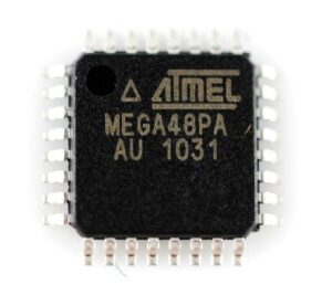
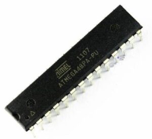
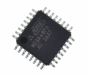
The phrase Read Microcontroller ATmega48PA Binary describes a practical, often necessary activity in embedded systems engineering: obtaining a firmware binary or heximal file from a physical MCU for legitimate purposes such as recovery, maintenance, or interoperability. The ATmega48PA, a member of Microchip’s AVR family, is a compact 8-bit microcontroller prized for low-power operation, versatile peripherals (timers, ADC, SPI, I²C/Two-Wire, UART), and a small on-chip flash and EEPROM region that stores the device program and calibration data. Because of its balance of capability and economy, the ATmega48PA appears across consumer electronics, portable instruments, hobbyist and educational platforms, low-volume industrial controllers, and some medical or measurement devices.
Why would anyone need to read microcontroller ATmega48PA binary? Legitimate reasons include recovering lost source code when repository backups are missing, duplicating an obsolete board for continued service, auditing a device’s firmware for safety or compliance, or restoring a device after component failure. In long-lived systems and regulated industries, being able to access a device’s archive of program data is essential to preserve functionality and assure continuity.
Read Microcontroller ATmega48PA Binary from its locked flash and eeprom, using focus ion beam to break mcu atmega48pa protective system and rewrite the firmware to new microcontroller atmega48pa for cloning;
All AVR ports have true Read-Modify-Write functionality when used as general digital I/O ports. This means that the direction of one port pin can be changed without unintentionally changing the direction of any other pin with the SBI and CBI instructions.
The same applies when changing drive value (if configured as output) or enabling/disabling of pull-up resistors (if configured as input). Each output buffer has symmetrical drive characteristics with both high sink and source capability. The pin driver is strong enough to drive LED displays directly. All port pins have individually selectable pull-up resistors with a supply-voltage invariant resistance.
All I/O pins have protection diodes to both VCC and Ground as indicated in Figure 12-1. Refer to ”Electrical Characteristics” on page 303 for a complete list of parameters when extracting atmega48 mikrocontroller heximal software. All registers and bit references in this section are written in general form. A lower case “x” represents the numbering letter for the port, and a lower case “n” represents the bit number.
However, when using the register or bit defines in a program, the precise form must be used. For example, PORTB3 for bit no. 3 in Port B, here documented generally as PORTxn. The physical I/O Registers and bit locations are listed in ”Register Description” on page 87.
Manufacturers commonly enable security measures to prevent unauthorized copying or tampering. The ATmega48PA supports lock features and configuration fuses that render the flash protected, locked, or otherwise inaccessible through standard programmer interfaces. As a result, efforts to crack, break, attack, hack, or decrypt protected firmware are technically and legally sensitive. Ethical and lawful practice requires that any attempt to recover, replicate, duplicate, or restore a protected file be done with explicit authorization from the device owner or under a clear legal framework.
The primary difficulties encountered when attempting to access a secured ATmega48PA dump are multifaceted:
-
Logical protections: Lock bits and fuse settings can disable normal readout commands, making straightforward copying impossible.
-
Physical constraints: Small packages, dense PCB layouts, and absent debug headers complicate non-destructive access to the chip’s programming lines.
-
Data interpretation: A raw binary or dump is compiled machine code; converting it back into human-readable source code or understanding proprietary protocols requires expert reverse engineering and familiarity with AVR instruction sets.
-
Risk to assets: Invasive attempts risk damaging the chip or board, potentially destroying the very archive intended for recovery.
-
Legal/ethical boundaries: Unauthorized attempts to clone or copy commercial firmware may violate copyright, licensing, or export controls.
Three I/O memory address locations are allocated for each port, one each for the Data Register – PORTx, Data Direction Register – DDRx, and the Port Input Pins – PINx. The Port Input Pins I/O location is read only, while the Data Register and the Data Direction Register are read/write.
However, writing a logic one to a bit in the PINx Register, will result in a toggle in the corresponding bit in the Data Register. In addition, the Pull-up Disable – PUD bit in MCUCR disables the pull-up function for all pins in all ports when set. Using the I/O port as General Digital I/O is described in ”Ports as General Digital I/O” on page 72. Most port pins are multiplexed with alternate functions for the peripheral features on the device to readout mcu atmega48v program from its flash memory. How each alternate function interferes with the port pin is described in ”Alternate Port Functions” on page 76. Refer to the individual module sections for a full description of the alternate functions.
Each port pin consists of three register bits: DDxn, PORTxn, and PINxn. As shown in ”Register Description” on page 87, the DDxn bits are accessed at the DDRx I/O address, the PORTxn bits at the PORTx I/O address, and the PINxn bits at the PINx I/O address.
The DDxn bit in the DDRx Register selects the direction of this pin. If DDxn is written logic one, Pxn is configured as an output pin. If DDxn is written logic zero, Pxn is configured as an input pin. If PORTxn is written logic one when the pin is configured as an input pin, the pull-up resistor is activated. To switch the pull-up resistor off, PORTxn has to be written logic zero or the pin has to be configured as an output pin. The port pins are tri-stated when reset condition becomes active, even if no clocks are running.
Because of these obstacles, the responsible path to obtain an ATmega48PA firmware binary is often non-technical: contact the original manufacturer for firmware or signed images, work under a maintenance contract, or obtain written permission from the rights holder. When technical analysis is required for legitimate security research, compliance testing, or product maintenance, professional reverse engineering services and careful documentation help preserve device safety and legal compliance.
In short, Read Microcontroller ATmega48PA Binary encapsulates an activity with real benefits for recovery and longevity of embedded products, but it must be balanced against the practical difficulties of protected memories and the legal/ethical imperative to avoid unauthorized cloning, copying, or misuse of secured firmware.