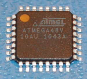
The ability to read MCU ATMEGA48V program from a secured or locked chip is a highly specialized task that lies at the intersection of hardware analysis, embedded security, and reverse engineering. The ATmega48V, produced by Microchip (formerly Atmel), is a low-power, high-performance 8-bit AVR microcontroller. With 4KB of in-system programmable flash, EEPROM, SRAM, and advanced peripherals, this MCU is widely deployed across industrial control, consumer electronics, medical devices, and automotive systems where reliability and efficiency are critical.
When companies need to recover lost firmware, restore legacy designs, or replicate discontinued hardware, accessing the original binary or heximal code stored inside the ATmega48V becomes essential. However, extracting this program is not straightforward once the chip has been configured with protection mechanisms.
The ATmega48V supports low-voltage operation (down to 1.8V), making it suitable for portable and battery-powered systems. It includes hardware features such as timers, ADC, SPI, I²C, and USART interfaces, enabling seamless integration into measurement instruments, wireless modules, and automotive electronic controls. In many cases, the firmware stored within the MCU represents years of development effort — proprietary source code, calibration data, or communication protocols. To prevent unauthorized copy or clone, device manufacturers enable lock bits that make the flash encrypted, protected, and inaccessible through standard programming interfaces.
Read MCU ATMEGA48V Program out from its flash memory after unlock Microcontroller ATmega48V encrypted memory and cut off the security fuse bit which is connected processor to memory.
Port B is an 8-bit bi-directional I/O port with internal pull-up resistors (selected for each bit). The Port B output buffers have symmetrical drive characteristics with both high sink and source capability. As inputs, Port B pins that are externally pulled low will source current if the pull-up resistors are activated. The Port B pins are tri-stated when a reset condition becomes active, even if the clock is not running.
Depending on the clock selection fuse settings, PB6 can be used as input to the inverting Oscillator amplifier and input to the internal clock operating circuit. Depending on the clock selection fuse settings, PB7 can be used as output from the inverting Oscillator amplifier.
If the Internal Calibrated RC Oscillator is used as chip clock source, PB7..6 is used as TOSC2..1 input for the Asynchronous Timer/Counter2 if the AS2 bit in ASSR is set before extract MCU embedded firmware.
Port C is a 7-bit bi-directional I/O port with internal pull-up resistors (selected for each bit). The PC5..0 output buffers have symmetrical drive characteristics with both high sink and source capability. As inputs, Port C pins that are externally pulled low will source current if the pull-up resistors are activated. The Port C pins are tri-stated when a reset condition becomes active, even if the clock is not running.
If the RSTDISBL Fuse is programmed, PC6 is used as an I/O pin. Note that the electrical characteristics of PC6 differ from those of the other pins of Port C. If the RSTDISBL Fuse is unprogrammed, PC6 is used as a Reset input. A low level on this pin for longer than the minimum pulse length will generate a Reset, even if the clock is not running.
Port D is an 8-bit bi-directional I/O port with internal pull-up resistors (selected for each bit). The Port D output buffers have symmetrical drive characteristics with both high sink and source capability. As inputs, Port D pins that are externally pulled low will source current if the pull-up resistors are activated. The Port D pins are tri-stated when a reset condition becomes active, even if the clock is not running.
To read MCU ATMEGA48V program from a locked device, engineers must employ advanced attack strategies. Common approaches include:
-
Decapsulation: Removing the protective packaging to expose the silicon die, enabling microprobing or laser fault injection to intercept memory operations.
-
Glitch attacks: Injecting clock or voltage irregularities to momentarily bypass security logic and access the flash dump.
-
Side-channel analysis: Measuring electromagnetic radiation or power consumption to decode internal processes and extract binary files indirectly.
-
Protocol exploitation: Identifying hidden or undocumented debug interfaces that can be leveraged to hack into the MCU.
Each of these methods carries risk. A failed attempt during chip-level attack may damage the MCU permanently, destroying the very firmware archive intended for recovery.
Challenges in Reverse Engineering ATmega48V
Unlike higher-capacity MCUs, the ATmega48V is compact, which makes direct microprobing or data line interception more difficult. Additionally, security fuse configurations can render the flash memory unreadable without invasive approaches. Even if the binary file is successfully extracted, engineers often need to decode and analyze the content to rebuild source code or verify program logic. This process requires extensive expertise in reverse engineering and familiarity with AVR instruction sets.
AVCC is the supply voltage pin for the A/D Converter, PC3:0, and ADC7:6. It should be externally connected to VCC, even if the ADC is not used. If the ADC is used, it should be connected to VCC through a low-pass filter. Note that PC6..4 use digital supply voltage, VCC before extract microcontroller atmega162v code.
In the TQFP and QFN/MLF package, ADC7:6 serve as analog inputs to the A/D converter. These pins are powered from the analog supply and serve as 10-bit ADC channels. The ATmega48V is a low-power CMOS 8-bit microcontroller based on the AVR enhanced RISC architecture.
The effort to read MCU ATMEGA48V program demonstrates the delicate balance between protecting intellectual property and ensuring that essential data can be recovered when necessary. For industries relying on long product lifecycles, the ability to replicate, duplicate, or restore embedded systems is invaluable. Yet, the task of cracking a secured ATmega48V remains highly complex, involving both hardware and software-level strategies. It is not just about copying a chip, but about carefully navigating the layers of security to preserve critical technological assets.