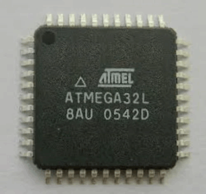
The ATMEGA32L is a popular 8-bit microcontroller from Atmel’s AVR family, widely used in embedded applications for its versatility, low power consumption, and rich feature set. It offers multiple I/O ports, built-in timers, ADC, USART communication, and extensive support for both flash and EEPROM memory. Due to its flexibility, it finds applications in industrial automation, consumer electronics, medical devices, automotive control systems, and smart appliances.
However, in many cases, the firmware stored inside an ATMEGA32L is protected, encrypted, or locked by fuse bits to prevent unauthorized copy or clone operations. While such security mechanisms are vital for safeguarding intellectual property, there are legitimate scenarios where it becomes necessary to read IC ATMEGA32L software—for example, restoring lost binary data, analyzing an archived program, or transferring a secured control system to new hardware.
Recovering the Heximal File from ATMEGA32L
The process of extracting a heximal or binary file from an ATMEGA32L involves specialized hardware and software tools to interface with the memory. By carefully disabling protection through controlled methods, it is possible to restore, decode, and unlock the content from both flash and EEPROM sections. This allows engineers to duplicate the program into a new microcontroller, modify it for system upgrades, or decrypt it for security auditing.
Common Steps in Breaking Protection and Disabling Fuse Bits
While exact methods vary depending on the level of security, the general process includes:
-
Device Identification – Confirming the exact chip model and reading its configuration bits.
-
Security Analysis – Checking fuse and lock bit settings to determine the type of protection.
-
Interface Setup – Connecting a high-precision programmer/debugger to the IC using ISP or high-voltage programming modes.
-
Protection Bypass – Using controlled voltage and clock manipulation techniques to temporarily bypass or reset security settings.
-
Data Extraction – Reading firmware, source code equivalent (via disassembly), or complete binary/heximal dump from flash and EEPROM memory.
-
Verification – Comparing extracted data against expected files or archives to ensure completeness.
These steps are performed with precision to avoid damaging the chip or corrupting the stored program.
Applications of Reading ATMEGA32L Firmware
Recovering the software from an ATMEGA32L can support a wide range of industries:
-
Manufacturing – Cloning machine control programs for backup or replication.
-
Maintenance – Restoring critical systems when original firmware is lost or damaged.
-
Security Audits – Analyzing code for vulnerabilities and ensuring compliance.
-
Product Development – Studying existing code to improve or integrate new features.
-
Education and Research – Learning microcontroller architecture by studying real-world embedded applications.
Unique Features of ATMEGA32L
The ATMEGA32L stands out for its low-voltage operation, ability to run at high speeds while consuming minimal power, and robust peripheral set. Its protected memory architecture allows developers to secure their code while still enabling legitimate recovery when necessary.
In conclusion, the ability to read IC ATMEGA32L software—including crack, hack, open, copy, and duplicate functions for protected firmware—provides a valuable tool for engineers, researchers, and maintenance professionals across industries. With the right expertise, even a secured ATMEGA32L can yield its binary secrets, ensuring that systems remain functional, adaptable, and secure.
Read IC ATMEGA32L Software can help engineer to recover MCU firmware in the format of heximal and clone IC functions to other blank Microcontroller ATmega32L through IC breaking technique;
Port A serves as the analog inputs to the A/D Converter.
Port A also serves as an 8-bit bi-directional I/O port, if the A/D Converter is not used. Port pins can provide internal pull-up resistors (selected for each bit). The Port A output buffers have symmetrical drive characteristics with both high sink and source capability.
When pins PA0 to PA7 are used as inputs and are externally pulled low, they will source current if the internal pull-up resistors are activated. The Port A pins are tri-stated when a reset condition becomes active, even if the clock is not running. Port B is an 8-bit bi-directional I/O port with internal pull-up resistors (selected for each bit). The Port B output buffers have symmetrical drive characteristics with both high sink and source capability. As inputs, Port B pins that are externally pulled low will source current if the pull-up resistors are activated. The Port B pins are tri-stated when a reset condition becomes active, even if the clock is not running after invasive mcu extraction.
Port C is an 8-bit bi-directional I/O port with internal pull-up resistors (selected for each bit). The Port C output buffers have symmetrical drive characteristics with both high sink and source capability. As inputs, Port C pins that are externally pulled low will source current if the pull-up resistors are activated. The Port C pins are tri-stated when a reset condition becomes active, even if the clock is not running.
If the JTAG interface is enabled, the pull-up resistors on pins PC5(TDI), PC3(TMS) and PC2(TCK) will be activated even if a reset occurs. Port D is an 8-bit bi-directional I/O port with internal pull-up resistors (selected for each bit). The Port D output buffers have symmetrical drive characteristics with both high sink and source capability. As inputs, Port D pins that are externally pulled low will source current if the pull-up resistors are activated. The Port D pins are tri-stated when a reset condition becomes active, even if the clock is not running if Read mcu at89c51cc03 flash.
In order to maximize performance and parallelism, the AVR uses a Harvard architecture – with separate memories and buses for program and data. Instructions in the program memory are executed with a single level pipelining. While one instruction is being executed, the next instruction is pre-fetched from the program memory.
This concept enables instructions to be executed in every clock cycle. The program memory is In-System Reprogrammable Flash memory. The fast-access Register File contains 32 x 8-bit general purpose working registers with a single clock cycle access time. This allows single-cycle Arithmetic Logic Unit (ALU) operation. In a typical ALU operation, two operands are output from the Register File, the operation is executed, and the result is stored back in the Register File – in one clock cycle.
Six of the 32 registers can be used as three 16-bit indirect address register pointers for Data Space addressing – enabling efficient address calculations. One of the these address pointers can also be used as an address pointer for look up tables in Flash Program memory. These added function registers are the 16-bit X-, Y-, and Z-register, described later in this section.
The ALU supports arithmetic and logic operations between registers or between a constant and a register. Single register operations can also be executed in the ALU. After an arithmetic operation, the Status Register is updated to reflect information about the result of the operation before Read mcu method.
Program flow is provided by conditional and unconditional jump and call instructions, able to directly address the whole address space. Most AVR instructions have a single 16-bit word format. Every program memory address contains a 16- or 32-bit instruction.
Program Flash memory space is divided in two sections, the Boot program section and the Application Program section. Both sections have dedicated Lock bits for write and read/write protection. The SPM instruction that writes into the Application Flash memory section must reside in the Boot Program section.
During interrupts and subroutine calls, the return address Program Counter (PC) is stored on the Stack. The Stack is effectively allocated in the general data SRAM, and consequently the Stack size is only limited by the total SRAM size and the usage of the SRAM. All user programs must initialize the SP in the reset routine (before subroutines or interrupts are executed). The Stack Pointer SP is read/write accessible in the I/O space. The data SRAM can easily be accessed through the five different addressing modes supported in the AVR architecture.