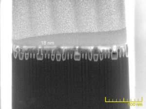
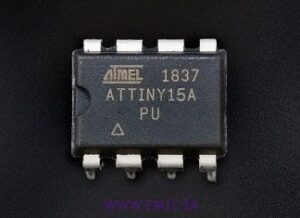
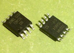
Extract IC ATtiny15 Software from its flash memory, crack attiny15 mcu fuse bit and clone embedded firmware to new microcontroller attiny15;
The ATtiny15L is a low-power CMOS 8-bit microcontroller based on the AVR RISC architecture. By executing powerful instructions in a single clock cycle, the ATtiny15L achieves throughputs approaching 1 MIPS per MHz allowing the system designer to optimize power consumption versus processing speed.
The AVR core combines a rich instruction set with 32 general purpose working registers. All the 32 registers are directly connected to the Arithmetic Logic Unit (ALU), allowing two independent registers to be accessed in one single instruction executed in one clock cycle if Extract IC.
The resulting architecture is more code efficient while achieving throughputs up to ten times faster than conventional CISC microcontrollers. The ATtiny15L provides 1K byte of Flash, 64 bytes EEPROM, six general purpose I/O lines, 32 general purpose working registers, two 8-bit Timer/Counters, one with high-speed PWM output, internal oscillators, internal and external interrupts, programmable Watchdog Timer, 4-channel 10-bit Analog-to-Digital Converter with one differential voltage input with optional 20x gain, and three software-selectable Power-saving modes.
The Idle mode stops the CPU while allowing the ADC, analog comparator, Timer/Counters and interrupt system to continue functioning. The ADC Noise Reduction mode facilitates high-accuracy ADC measurements by stopping the CPU while allowing the ADC to continue functioning. The Power-down mode saves the register contents but freezes the oscillators, disabling all other chip functions until the next interrupt or hardware reset. The wake-up or interrupt on pin change features enable the ATtiny15L to be highly responsive to external events, still featuring the lowest power consumption while in the Power-saving modes after Extract IC.
The device is manufactured using Atmel’s high-density, nonvolatile memory technology. By combining a RISC 8-bit CPU with Flash on a monolithic chip, the ATtiny15L is a powerful microcontroller that provides a highly flexible and cost-efficient solution to many embedded control applications. The peripheral features make the ATtiny15L particularly suited for battery chargers, lighting ballasts and all kinds of intelligent sensor applications.
The ATtiny15L AVR is supported with a full suite of program and system development tools including macro assemblers, program debugger/simulators, In-circuit emulators and evaluation kits. Port B is a 6-bit I/O port. PB4..0 are I/O pins that can provide internal pull-ups (selected for each bit). PB5 is input or open-drain output. The use of pin PB5 is defined by a fuse and the special function associated with this pin is external Reset.
The port pins are tristated when a reset condition becomes active, even if the clock is not running. The internal oscillator provides a clock rate of nominally 1.6 MHz for the system clock (CK). Due to large initial variation (0.8 -1.6 MHz) of the internal oscillator, a tuning capability is built in. Through an 8-bit control register – OSCCAL – the system clock rate can be tuned with less than 1% steps of the nominal clock.
There is an internal PLL that provides a 16x clock rate locked to the system clock (CK) for the use of the Peripheral Timer/Counter1. The nominal frequency of this peripheral clock, PCK, is 25.6 MHz. The fast-access register file concept contains 32 x 8-bit general purpose working registers with a single-clock-cycle access time. This means that during one single clock cycle, one ALU (Arithmetic Logic Unit) operation is executed.
Two operands are output from the register file, the operation is executed, and the result is stored back in the register file – in one clock cycle. Two of the 32 registers can be used as a 16-bit pointer for indirect memory access. This pointer is called the Z-pointer, and can address the register file, IO file and the Flash program memory.