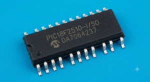
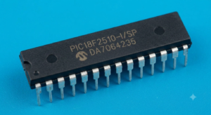
The resilience of an automated production line frequently depends on the longevity of its embedded microcomponents. When an legacy system faces unexpected hardware degradation and the original blueprints are completely missing, the capability to copy protected mcu pic18f2510 heximal arrays becomes a cornerstone of industrial survival. The pic18f2510 is a highly integrated 28-pin flash-based microcontroller featuring an advanced 10-bit analog-to-digital converter (adc), multiple high-speed capture/compare/pwm (ccp) modules, and a highly optimized internal oscillator block capable of executing precise timing commands.
Thanks to these versatile hardware capabilities, engineering teams traditionally deployed this rugged microprocessor inside remote telemetry devices, smart power-distribution grids, commercial aviation sub-panels, and sophisticated dental imaging equipment. When these complex fields experience an unpredictable system crash, technicians must find a non-destructive way to safely analyze the inner silicon structures to maintain global operational uptime.
The IDLEN bit determines if the device goes into Sleep mode or one of the Idle modes when the SLEEP instruction is executed. The use of the flag and control bits in the OSCCON register is discussed in more detail in Section 3.0 “Power Managed Modes”.
Note 1: The Timer1 oscillator must be enabled to select the secondary clock source. The Timer1 oscillator is enabled by setting the T1OSCEN bit in the Timer1 Control register (T1CON<3>). If the Timer1 oscillator is not enabled, then any attempt to select a secondary clock source will be ignored.
2: It is recommended that the Timer1 oscillator be operating and stable before selecting the secondary clock source or a very long delay may occur while the Timer1 oscillator starts. PIC18F2510 devices contain circuitry to prevent clock “glitches” when switching between clock sources. A short pause in the device clock occurs during the clock switch. The length of this pause is the sum of two cycles of the old clock source and three to four cycles of the new clock source. This formula assumes that the new clock source is stable. When PRI_IDLE mode is selected, the designated primary oscillator continues to run without interruption. For all other power managed modes, the oscillator using the OSC1 pin is disabled. The OSC1 pin (and OSC2 pin, if used by the oscillator) will stop oscillating. In secondary clock modes (SEC_RUN and SEC_IDLE), the Timer1 oscillator is operating and providing the device clock. The Timer1 oscillator may also run in all power managed modes if required to clock Timer1 or Timer3.
In internal oscillator modes (RC_RUN and RC_IDLE), the internal oscillator block provides the device clock source. The 31 kHz INTRC output can be used directly to provide the clock and may be enabled to support various special features, regardless of the power managed mode (see Section 23.2 “Watchdog Timer (WDT)”, Section 23.3 “Two-Speed Start-up” and Section 23.4 “Fail-Safe Clock Monitor” for more information on WDT, Fail-Safe Clock Monitor and Two-Speed Start-up). The INTOSC output at 8 MHz may be used directly to clock the device or may be divided down by the postscaler. The INTOSC output is disabled if the clock is provided directly from the INTRC output. If the Sleep mode is selected, all clock sources are stopped. Since all the transistor switching currents have been stopped, Sleep mode achieves the lowest current consumption of the device (only leakage currents).

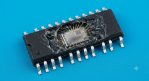
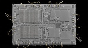
To extract machine code from a secured or locked semiconductor architecture, specialists must navigate a labyrinth of hardware-level defense arrays. The principal obstacle when trying to hack or open an encrypted component involves bypassing the active security fuse bits that block standard programming interfaces. The microcontroller leverages internal monitoring networks that track supply voltage fluctuations and clock frequency anomalies to detect unauthorized read commands, which can instantly trigger a total erase of the internal flash program memory and the adjacent eeprom cells. Safely circumventing these protective layers requires specialized signal injection tools designed to temporarily destabilize the defense logic without destroying the underlying silicon. Once these barriers are neutralized, engineers can safely execute a full memory dump, capturing the raw binary or heximal file that contains the necessary machine code to restore and replicate the system’s operational logic.
Reclaiming this hidden data archive is a vital strategic endeavor that goes far beyond simple curiosity. When original equipment manufacturers stop supporting older hardware generations, declare bankruptcy, or refuse to share legacy control files, companies often face a forced, multi-million dollar infrastructure overhaul. Having an uninhibited window into the system’s operational logic provides a definitive shield against vendor lock-in and supply chain vulnerabilities. It gives engineering departments the freedom to repair failing electronics, optimize legacy equipment for modern efficiency standards, and ensure strict long-term compliance. This precise technical capability effectively converts an impenetrable, depreciating hardware liability back into a fully visible, documented corporate asset, ensuring that the critical machine behavior is preserved without needing the manufacturer’s original source code.
Ultimately, obtaining a flawless heximal or binary file from a protected integrated circuit yields profound commercial benefits for our clients. By moving through a rigorously managed hardware reverse engineering cycle, corporate asset managers can effectively insulate themselves against forced platform migration and predatory vendor lock-in. Having a clean, verifiable copy of the mcu code grants internal development teams the power to audit legacy algorithms, clone end-of-life components onto highly sustainable circuit paths, and implement crucial cyber-security patches without redesigning the architecture from zero. This proactive technical capability successfully changes an unreadable, locked hardware barrier back into a completely transparent, well-documented software asset—drastically lowering operational overhead, bypassing unpredictable global logistics constraints, and guaranteeing business continuity for years to come.