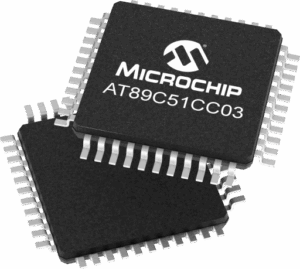
Read MCU AT89C51CC03 Program from its embedded memory have to remove the security fuse bit by focus ion beam, which is a key technology for microcontroller unlocking.
Some instructions read the latch data rather than the pin data. The latch based instructions read the data, modify the data and then rewrite the latch. These are called “Read-Modify-Write” instructions. Below is a complete list of these special instructions (see Table ). When the destination operand is a Port or a Port bit, these instructions read the latch rather than the pin when extract MCU at89c52 heximal:
It is not obvious the last three instructions in this list are Read-Modify-Write instructions. These instructions read the port (all 8 bits), modify the specifically addressed bit and write the new byte back to the latch. These Read-Modify-Write instructions are directed to the latch rather than the pin in order to avoid possible misinterpretation of voltage (and therefore, logic) levels at the pin.
For example, a Port bit used to drive the base of an external bipolar transistor can not rise above the transistor’s base-emitter junction voltage (a value lower than VIL). With a logic one written to the bit, attempts by the CPU to read the Port at the pin are misinterpreted as logic zero. A read of the latch rather than the pins returns the correct logic-one value.
Port 1, Port 2, Port 3 and Port 4 have fixed internal pull-ups and are referred to as “quasi-bidirectional” Ports. When configured as an input, the pin impedance appears as logic one and sources current in response to an external logic zero condition. Port 0 is a “true bidirectional” pin. The pins float when configured as input. Resets write logic one to all Port latches. If logical zero is subsequently written to a Port latch, it can be returned to input conditions by a logical one written to the latch.
Port latch values change near the end of Read-Modify-Write instruction cycles. Output buffers (and therefore the pin state) update early in the instruction after Read-Modify-Write instruction cycle. Logical zero-to-one transitions in Port 1, Port 2, Port 3 and Port 4 use an additional pull up (p1) to aid this logic transition (see Figure 4.). This increases switch speed. This extra pull-up sources 100 times normal internal circuit current during 2 oscillator clock periods. The internal pull-ups are field-effect transistors rather than linear resistors.
Pull-ups consist of three p-channel FET (pFET) devices. A pFET is on when the gate senses logical zero and off when the gate senses logical one. pFET #1 is turned on for two oscillator periods immediately after a zero-to-one transition in the Port latch. A logical one at the Port pin turns on pFET #3 (a weak pull-up) through the inverter. This inverter and pFET pair form a latch to drive logical one. pFET #2 is a very weak pull-up switched on whenever the associated nFET is switched off. This is traditional CMOS switch convention when copy chip embedded firmware.
Otro enfoque consiste en hackear el firmware mediante métodos basados en exploits, donde se utilizan vulnerabilidades en el gestor de arranque o el mecanismo de actualización del firmware del MCU para descifrar, decodificar o copiar los datos del programa. En algunos casos, los ingenieros pueden replicar, clonar o duplicar el código fuente analizando el archivo binario o de memoria recuperado del chip.
Current strengths are 1/10 that of pFET #3. The X2 bit in the CKCON register (see Table 2) allows switching from 12 clock cycles per instruction to 6 clock cycles and vice versa. At reset, the standard speed is activated (STD mode). Setting this bit activates the X2 feature (X2 mode) for the CPU Clock only.
The Timers 0, 1 and 2, Uart, PCA, WatchDog or CAN switch in X2 mode only if the corresponding bit is cleared in the CKCON register. The clock for the whole circuit and peripheral is first divided by two before being used by the CPU core and peripherals. This allows any cyclic ratio to be accepted on the XTAL1 input. In X2 mode, as this divider is bypassed, the signals on XTAL1 must have a cyclic ratio between 40 to 60%. Figure 5. shows the clock generation block diagram.
The X2 bit is validated on the XTAL1÷2 rising edge to avoid glitches when switching from the X2 to the STD mode. Figure 6 shows the mode switching waveforms.