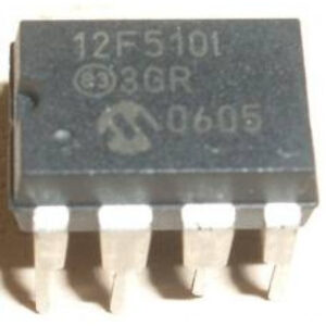
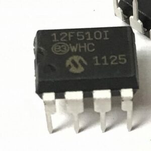
Copy Microcontroller PIC12F510 Program and data from its flash memory and eeprom memory separately out and reprogramme the code to blank MCU PIC12F510, reverse engineering microcontroller to acquire the circuitry pattern:

The EUSART supports 9-bit character reception. When the RX9 bit of the RCSTA register is set the EUSART will shift 9-bits into the RSR for each character received. The RX9D bit of the RCSTA register is the ninth, and Most Significant, data bit of the top unread character in the receive FIFO when read protect pic16f887 heximal.
When reading 9-bit data from the receive FIFO buffer, the RX9D data bit must be read before reading the 8 Least Significant bits from the RCREG.

- Initialize the SPBRGH, SPBRG register pair for the appropriate baud rate. Set or clear the BRGH and BRG16 bits, as required, to achieve the desired baud rate.
- Enable the synchronous master serial port by setting bits SYNC, SPEN and CSRC.
- Ensure bits CREN and SREN are clear.
- If using interrupts, set the GIE and PEIE bits of the INTCON register and set RCIE.
- If 9-bit reception is desired, set bit RX9.
- Start reception by setting the SREN bit or for continuous reception, set the CREN bit after extract secured mcu pic16lf88 flash.
- Interrupt flag bit RCIF will be set when reception of a character is complete. An interrupt will be generated if the enable bit RCIE was set.
- Read the RCSTA register to get the ninth bit (if enabled) and determine if any error occurred during reception.
- Read the 8-bit received data by reading the RCREG register.
- If an overrun error occurs, clear the error by either clearing the CREN bit of the RCSTA register or by clearing the SPEN bit which resets the EUSART when reading out mcu pic16f88 flash.
Setting the SYNC bit of the TXSTA register configures the device for synchronous operation. Clearing the CSRC bit of the TXSTA register configures the device as a slave.
Clearing the SREN and CREN bits of the RCSTA register ensures that the device is in the Transmit mode, otherwise the device will be configured to receive. Setting the SPEN bit of the RCSTA register enables the EUSART. If the RX/DT or TX/CK pins are shared with an analog peripheral the analog I/O functions must be disabled by clearing the corresponding ANSEL bits.

