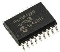
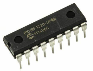
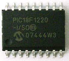
Unlock Secured PIC18F1220 Microprocessor Flash Memory and extract embedded heximal data from MCU PIC18F1220, copy binary firmware to new microcontroller PIC18F1220 which can be served as original one;
There are two memory blocks in each of these PICmicro® microcontroller devices. Each block (Program Memory and Data Memory) has its own bus so that concurrent access can occur which provide necessity for Break Microcontroller PIC16C716 Heximal.
The PIC18f1220 has a 13-bit program counter capable of addressing an 8K x 14 program memory space. PIC18F1220 has 1K x 14 words of program memory and PIC18f1220 has 2K x 14 words of program memory. Accessing a location above the physically implemented address will cause a wraparound.
Each bank extends up to 7Fh (128 bytes). The lower locations of each bank are reserved for the Special
Function Registers. Above the Special Function Registers are General Purpose Registers, implemented as static RAM. All implemented banks contain special function registers when reading out PIC18F46J50 microcontroller eeprom program. Some “high use” special function registers from one bank may be mirrored in another bank for code reduction and quicker access.
The Special Function Registers are registers used by the CPU and Peripheral Modules for controlling the desired operation of the device.
The special function registers can be classified into two sets; core (CPU) and peripheral. Those registers associated with the core functions are described in detail in this section. Those related to the operation of the peripheral features are described in detail in that peripheral feature section.
If the STATUS register is the destination for an instruction that affects the Z, DC or C bits, then the write to these three bits is disabled. These bits are set or cleared according to the device logic to copy microprocessor pic18f14k50 memory heximal. Furthermore, the TO and PD bits are not writable. Therefore, the result of an instruction with the STATUS register as destination may be different than intended.