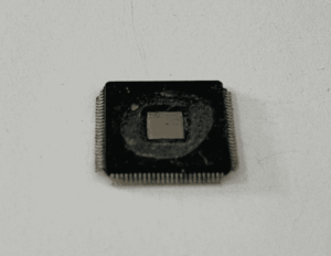
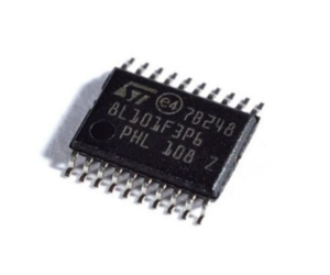
We can help engineer to break STM8L101F3P6 microcontroller security fuse bit and execute STMicroelectronics STM8L101F3P6 MCU Flash Code Extraction, and then clone stm8l101f3p6 ic mcu flash code;
Each power supply pair (VDD/VSS, VDDA/VSSA etc.) must be decoupled with filtering ceramic capacitors as shown above. These capacitors must be placed as close as possible to, or below, the appropriate pins on the underside of the PCB to ensure the good functionality of the device.
Stresses above the absolute maximum ratings listed in Table 12: Voltage characteristics, Table 13: Current characteristics: Thermal characteristics may cause permanent damage to the device. These are stress ratings only and functional operation of the device at these conditions is not implied when copy protective stm8s103f3p3 microprocessor flash heximal. Exposure to maximum rating conditions for extended periods may affect device reliability.
All main power (VDD, VDDA) and ground (VSS, VSSA) pins must always be connected to the external power supply, in the permitted range.
This current consumption must be correctly distributed over all I/Os and control The total output current must not be sunk/sourced between two consecutive power supply pins referring to high pin count QFP packages.
Positive injection is not possible on these I/Os and does not occur for input voltages lower than the specified maximum A positive injection is induced by VIN>VDD while a negative injection is induced by VIN<VSS. IINJ(PIN) must never be Refer to Table 12: Voltage characteristics for the maximum allowed input voltage values.
A positive injection is induced by VIN>VDDA while a negative injection is induced by VIN<VSS. IINJ(PIN) must never be Refer also to Table 12: Voltage characteristics for the maximum allowed input voltage values. Negative injection disturbs the analog performance of the device. See note (2) below Table 51: ADC accuracy.
When several inputs are submitted to a current injection, the maximum SIINJ(PIN) is the absolute sum of the positive and negative injected currents (instantaneous values).