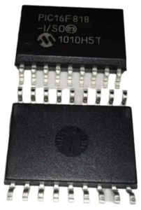
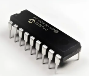
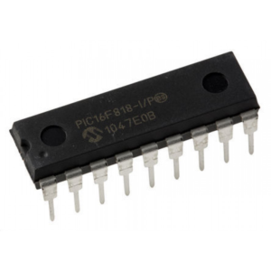
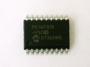
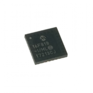
The PIC16F818 is a compact yet capable MCU widely used in embedded systems where cost, reliability, and low power consumption are critical. Built on an 8-bit architecture, this microcontroller integrates flash program memory, EEPROM for non-volatile data storage, timers, ADC modules, and communication peripherals, making it suitable for applications such as industrial controllers, consumer electronics, automotive subsystems, and IoT devices. Its balanced design allows engineers to deploy it in environments where stable firmware execution and efficient memory usage are essential. Because of its versatility, the chip often becomes a core component in products that require long-term reliability, including sensor interfaces, home automation devices, and portable instrumentation.
Mühendisler ve analistler, bakım, ürün yaşam döngüsü desteği veya uyumluluk geliştirme gibi meşru amaçlar için Microchip PIC16F818 mikrodenetleyicisinin program verilerini okumaya ihtiyaç duyabilirler. Bu genellikle, güvenli, korumalı veya hatta kilitli bir Microchip PIC16F818 MCU’dan bellenimi ayıklama, kurtarma veya geri yükleme girişimlerini içerir. Dahili flaş, EEPROM ve genel bellek, yıllarca süren geliştirme çabasını temsil eden Microchip PIC16F818 mikrodenetleyicisinin değerli ikili, onaltılık veya derlenmiş program dosyası yapılarını içerebilir. Orijinal dokümantasyon veya kaynak kodunun bulunmadığı durumlarda, profesyoneller depolanan veri arşivini veya Microchip PIC16F818 MCU dökümünü açmak ve yorumlamak için üst düzey tersine mühendislik yaklaşımlarına güvenebilirler. Bu süreçler, özellikle eski sistemler, üretimi durdurulmuş ürünler veya donanımın onarılması gereken ancak orijinal Microchip PIC16F818 mikroişlemcisinin bellenim yedeklerinin eksik olduğu durumlarda önemlidir. Daha da önemlisi, modern Microchip PIC16F818 mikroçiplerinde genellikle şifrelenmiş veya okuma korumalı bölgeler bulunur; bu da ürün yazılımına doğrudan erişimi önemli ölçüde daha karmaşık hale getirir ve özel uzmanlık ve araçlar gerektirir.
In many real-world scenarios, engineers and analysts may need to read microcontroller PIC16F818 program data for legitimate purposes such as maintenance, product lifecycle support, or compatibility development. This often involves attempts to extract, recover, or restore firmware from a secured, protected, or even locked chip. The internal flash, EEPROM, and overall memory may contain valuable binary, heximal, or compiled program file structures that represent years of development effort. In cases where original documentation or source code is unavailable, professionals may rely on high-level reverse engineering approaches to open and interpret the stored data archive or MCU dump. These processes are particularly relevant when dealing with legacy systems, discontinued products, or situations where hardware must be repaired but firmware backups are missing. Importantly, modern chips often include encrypted or read-protected regions, making direct access to the firmware significantly more complex and requiring specialized expertise and tools.
Engenheiros e analistas podem precisar ler os dados de programa do microcontrolador Microchip PIC16F818 para fins legítimos, como manutenção, suporte ao ciclo de vida do produto ou desenvolvimento de compatibilidade. Isso geralmente envolve tentativas de extrair, recuperar ou restaurar o firmware de um MCU Microchip PIC16F818 seguro, protegido ou até mesmo bloqueado. A memória flash interna, a EEPROM e a memória em geral podem conter estruturas de arquivos de programa binários, hexadecimais ou compilados valiosos do microcontrolador Microchip PIC16F818, que representam anos de desenvolvimento. Nos casos em que a documentação original ou o código-fonte não estão disponíveis, os profissionais podem recorrer a abordagens de engenharia reversa de alto nível para abrir e interpretar o arquivo de dados armazenado ou o dump do MCU Microchip PIC16F818. Esses processos são particularmente relevantes ao lidar com sistemas legados, produtos descontinuados ou situações em que o hardware precisa ser reparado, mas os backups originais do firmware do microprocessador Microchip PIC16F818 estão ausentes. É importante destacar que os microchips PIC16F818 modernos da Microchip geralmente incluem regiões criptografadas ou protegidas contra leitura, o que torna o acesso direto ao firmware significativamente mais complexo e exige conhecimento e ferramentas especializadas.
PORTD is an 8-bit port with Schmitt Trigger input buffers. Each pin is individually configureable as an input or output. PORTD can be configured as an 8-bit wide microprocessor port (parallel slave port) by setting control bit PSPMODE (TRISE<4>). In this mode, the input buffers are TTL.
This section is not applicable to the PIC16F818.
PORTE has three pins, RE0/RD/AN5, RE1/WR/AN6 and RE2/CS/AN7, which are individually configureable as inputs or outputs. These pins have Schmitt Trigger I/O PORTE becomes control inputs for the microprocessor port when bit PSPMODE (TRISE<4>) is set.
In this mode, the user must make sure that the TRISE<2:0> bits are set (pins are configured as digital inputs). Ensure ADCON1 is configured for digital I/O.
In this mode, the input buffers are TTL. Register 4-1 shows the TRISE register, which also controls the parallel slave port operation. PORTE pins are multiplexed with analog inputs.
Inżynierowie i analitycy mogą potrzebować odczytać dane programu mikrokontrolera Microchip PIC16F818 do uzasadnionych celów, takich jak konserwacja, wsparcie cyklu życia produktu lub rozwój zgodności. Często wiąże się to z próbami wyodrębnienia, odzyskania lub przywrócenia oprogramowania sprzętowego z zabezpieczonego, chronionego, a nawet zablokowanego mikrokontrolera Microchip PIC16F818. Wewnętrzna pamięć flash, EEPROM i pamięć ogólna mogą zawierać cenne binarne, heksagonalne lub skompilowane struktury plików programu mikrokontrolera Microchip PIC16F818, które odzwierciedlają lata wysiłków rozwojowych. W przypadkach, gdy oryginalna dokumentacja lub kod źródłowy są niedostępne, specjaliści mogą polegać na podejściach inżynierii wstecznej wysokiego poziomu, aby otworzyć i zinterpretować zapisane archiwum danych lub zrzut pamięci mikrokontrolera Microchip PIC16F818. Procesy te są szczególnie istotne w przypadku starszych systemów, wycofanych produktów lub sytuacji, w których sprzęt musi zostać naprawiony, ale brakuje oryginalnych kopii zapasowych oprogramowania sprzętowego mikroprocesora Microchip PIC16F818. Co ważne, nowoczesne mikroprocesory Microchip PIC16F818 często zawierają szyfrowane lub chronione przed odczytem obszary, co znacznie utrudnia bezpośredni dostęp do oprogramowania sprzętowego i wymaga specjalistycznej wiedzy oraz narzędzi.
When selected as an analog input, these pins will read as ’0’s. TRISE controls the direction of the RE pins, even when they are being used as analog inputs. The user must make sure to keep the pins configured as inputs when using them as analog inputs. The Parallel Slave Port (PSP) is not implemented on the PIC16F818. PORTD operates as an 8-bit wide Parallel Slave Port, or Microprocessor Port, when control bit PSPMODE (TRISE<4>) is set. In Slave mode, it is asynchronously readable and writable by an external system using the read control input pin RE0/RD. the write control input pin RE1/WR, and the chip select control input pin RE2/CS.
Inženýři a analytici mohou potřebovat číst programová data mikrokontroléru Microchip PIC16F818 pro legitimní účely, jako je údržba, podpora životního cyklu produktu nebo vývoj kompatibility. To často zahrnuje pokusy o extrahování, obnovu nebo obnovení firmwaru ze zabezpečeného, chráněného nebo dokonce uzamčeného mikrokontroléru Microchip PIC16F818. Interní flash, EEPROM a celková paměť mohou obsahovat cenné binární, heximální nebo kompilované struktury programových souborů mikrokontroléru Microchip PIC16F818, které představují roky vývojového úsilí. V případech, kdy není k dispozici originální dokumentace nebo zdrojový kód, se profesionálové mohou spolehnout na přístupy reverzního inženýrství na vysoké úrovni k otevření a interpretaci uloženého archivu dat nebo výpisu dat mikrokontroléru Microchip PIC16F818. Tyto procesy jsou obzvláště důležité při práci se staršími systémy, ukončenými produkty nebo v situacích, kdy je nutné opravit hardware, ale chybí původní zálohy firmwaru mikroprocesoru Microchip PIC16F818. Důležité je, že moderní mikročipy Microchip PIC16F818 často obsahují šifrované nebo proti čtení chráněné oblasti, což výrazně ztěžuje přímý přístup k firmwaru a vyžaduje specializované znalosti a nástroje.
Ultimately, the ability to analyze and retrieve firmware from embedded systems provides tangible benefits. It enables product repair, extends the lifespan of electronic devices, supports interoperability, and facilitates innovation through deeper understanding of existing designs. For clients, this can translate into reduced costs, minimized downtime, and preservation of valuable intellectual assets. Whether the goal is to restore a malfunctioning device, archive critical data, or perform high-level reverse engineering for compatibility, the process plays an important role in modern electronics support and research. While respecting legal and ethical boundaries is essential, the controlled study of microcontroller firmware continues to be a meaningful practice in advancing embedded technology and ensuring long-term system sustainability.
Инженерам и аналитикам может потребоваться чтение программных данных микроконтроллера Microchip PIC16F818 в законных целях, таких как техническое обслуживание, поддержка жизненного цикла продукта или разработка совместимости. Часто это включает попытки извлечения, восстановления или восстановления микропрограммного обеспечения из защищенного, охраняемого или даже заблокированного микроконтроллера Microchip PIC16F818. Внутренняя флэш-память, EEPROM и общая память могут содержать ценные двоичные, шестнадцатеричные или скомпилированные структуры программных файлов микроконтроллера Microchip PIC16F818, представляющие собой результат многолетней работы по разработке. В случаях, когда оригинальная документация или исходный код недоступны, специалисты могут использовать высокоуровневые методы обратного проектирования для открытия и интерпретации архива хранимых данных или дампа микроконтроллера Microchip PIC16F818. Эти процессы особенно актуальны при работе с устаревшими системами, снятыми с производства продуктами или в ситуациях, когда необходимо отремонтировать оборудование, но отсутствуют резервные копии микропрограммного обеспечения оригинального микропроцессора Microchip PIC16F818. Важно отметить, что современные микроконтроллеры Microchip PIC16F818 часто содержат зашифрованные или защищенные от чтения области, что значительно усложняет прямой доступ к встроенному программному обеспечению и требует специальных знаний и инструментов.