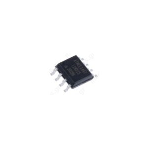
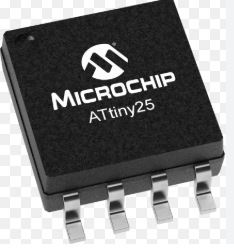
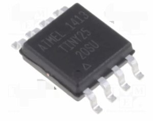
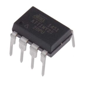
Read Microcontroller ATtiny25 Flash describes a focused, professional service: extracting the compiled program image and related data that live inside a small, low‑power AVR microcontroller so organizations can recover, preserve, or validate deployed systems. The ATtiny25 is a compact 8‑bit MCU with limited on‑chip flash and EEPROM but a surprisingly capable peripheral set—ADC channels, timers, a serial interface and multiple power‑saving modes—making it a popular choice for battery‑powered sensors, compact user interfaces, wearable controls, toys and simple industrial sensors. These technical traits explain why designers embed important program logic and calibration data in its flash and EEPROM.
Read Microcontroller ATtiny25 Flash and crack attiny25 microcontroller security fuse bit then recover embedded heximal from locked MCU to new attiny25;
The ATtiny25/45/85 is a low-power CMOS 8-bit microcontroller based on the AVR enhanced RISC architecture. By executing powerful instructions in a single clock cycle, the ATtiny25/45/85 achieves throughputs approaching 1 MIPS per MHz allowing the system designer to optimize power consumption versus processing speed.
In practice, reading the MCU’s flash is rarely done for nefarious reasons. Companies commonly need to recover a binary or hex file when source repositories are lost, to restore a device after a failed update, or to archive firmware for long‑term support. A clean dump of program memory becomes the starting point for lawful reverse engineering, firmware validation, or to reproduce a discontinued unit that is critical to a production line. The recovered file serves as an auditable archive so engineers can verify control logic, re‑create firmware images, or supply compatible spare modules to fielded equipment.
Manufacturers intentionally provide mechanisms to protect program memory: lock‑bits, fuse settings and programming modes that block ordinary readout are standard features. In some cases the datasheet documents high‑voltage programming and lock behavior that prevent casual copying; these protections help safeguard intellectual property but also create legitimate maintenance challenges for owners who lost access to original source code. Responsible recovery work respects those protections — obtaining explicit authorization, maintaining chain‑of‑custody documentation and avoiding publication of methods that would enable unauthorized cloning.
The AVR core combines a rich instruction set with 32 general purpose working registers. All the 32 registers are directly connected to the Arithmetic Logic Unit (ALU), allowing two independent registers to be accessed in one single instruction executed in one clock cycle.
Technically, the ATtiny25’s constrained memory footprint shapes the complexity of any recovery effort. A typical ATtiny25 program image is compact and highly optimized; a dumped binary is dense and devoid of symbols or comments, so interpreting it to reconstruct meaningful behavior requires skilled analysis of AVR instruction flow, data tables and peripheral interactions. On the hardware side, the small package and compact PCB layouts common in ATtiny25 applications can hide debug pads and make non‑destructive access challenging. Any extraction attempt must be designed to preserve EEPROM calibration data and avoid corrupting the device.
The resulting architecture is more code efficient while achieving throughputs up to ten times faster than conventional CISC microcontrollers.
The ATtiny25/45/85 provides the following features: 2/4/8K byte of In-System Programmable Flash, 128/256/512 bytes EEPROM, 128/256/256 bytes SRAM, 6 general purpose I/O lines, 32 general purpose working registers, one 8-bit Timer/Counter with compare modes when reading microcontroller attiny25 flash content file, one 8-bit high speed Timer/Counter, Universal Serial Interface, Internal and External Interrupts, a 4-channel, 10-bit ADC, a programmable Watchdog Timer with internal Oscillator, and three software selectable power saving modes.
The Idle mode stops the CPU while allowing the SRAM, Timer/Counter, ADC, Analog Comparator, and Interrupt system to continue functioning. The Power-down mode saves the register contents, disabling all chip functions until the next Interrupt or Hardware Reset.
The ADC Noise Reduction mode stops the CPU and all I/O modules except ADC, to minimize switching noise during ADC conversions. The device is manufactured using Atmel’s high density non-volatile memory technology.
The On-chip ISP Flash allows the Program memory to be re-programmed In-System through an SPI serial interface, by a conventional non-volatile memory programmer or by an On-chip boot code running on the AVR core.
The ATtiny25/45/85 AVR is supported with a full suite of program and system development tools including: C Compilers, Macro Assemblers, Program Debugger/Simulators, In-Circuit Emulators, and Evaluation kits.
Why do clients invest in this capability? The benefits are practical and measurable: faster repairs through re‑flashing, reduced field downtime, validated archives for compliance and safety audits, and the ability to lawfully replicate or restore legacy modules when the original vendor disappears. For organizations with long product lifecycles, a verified program archive protects intellectual property value and keeps critical systems operational. Importantly, these outcomes are delivered under clear authorization and with robust documentation to protect client IP and customer data.
In summary, Read Microcontroller ATtiny25 Flash is a high‑value, sensitive service that combines embedded‑systems expertise, careful reverse engineering, and legal safeguards. When performed correctly, it converts a locked, inaccessible program and data archive into a controlled, auditable asset—enabling maintenance, compliance, and long‑term product continuity while protecting the owner’s rights and safety.