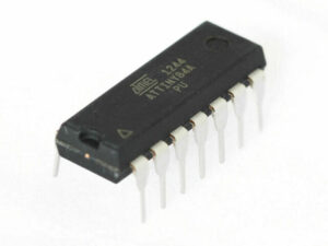
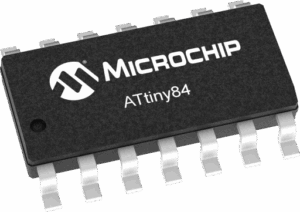
Read IC ATtiny84A Firmware describes a professional, authorized process for retrieving the compiled program image and associated data stored inside a small AVR microcontroller so companies can recover, validate, or maintain deployed systems. The ATtiny84A is prized for its compact footprint, modest flash and EEPROM, versatile timers and ADC channels, and low-power modes. Those characteristics make it a common choice for battery-powered sensors, compact user interfaces, LED drivers, portable instrumentation, and a wide range of consumer and light-industrial products where space and energy efficiency are priorities.
In real products the flash of an ATtiny84A frequently holds more than simple control logic. Calibration tables, communication stacks, configuration records and proprietary program routines are all commonly embedded alongside persistent data in EEPROM. When original source repositories are lost or a field update corrupts a device, obtaining a faithful binary or hex dump of the firmware archive becomes the starting point to restore function. That recovered file lets engineers analyze program flow, verify safety controls, or create a tested replacement module while preserving the integrity of the device’s memory.
Read MCU ATtiny84A Binary needs to break microcontroller attiny84A protective system and then unlock embedded firmware from attiny84A flash and eeprom memory;
The internal oscillator provides a clock rate of nominally 1.6 MHz for the system clock (CK). Due to large initial variation (0.8 -1.6 MHz) of the internal oscillator, a tuning capability is built in. Through an 8-bit control register – OSCCAL – the system clock rate can be tuned with less than 1% steps of the nominal clock.
There is an internal PLL that provides a 16x clock rate locked to the system clock (CK) for the use of the Peripheral Timer/Counter1. The nominal frequency of this peripheral clock, PCK, is 25.6 MHz.
Because vendors often enable protections to prevent unauthorized cloning or copying, reading a protected, locked, or encrypted region of on-chip memory is intentionally difficult. Conversations about this technology sometimes use charged verbs — crack, break, attack, hack, decrypt — but responsible practitioners avoid describing methods in public. Instead the focus is on lawful recovery: non-destructive extraction, careful interpretation of the binary, and validated restoration or replication only under clear authorization. Reverse engineering in this context means translating a raw dump into meaningful insights without facilitating misuse.
The ATtiny84A’s constrained resources shape both the technical challenge and the value of recovery. Small, optimized programs produce dense binaries that lack symbols or comments; decoding that machine code into understandable logic requires experience with AVR instruction sets and careful forensic analysis. Physically, tiny packages and crowded PCBs can hide debug contacts and make non-invasive access harder; any invasive attempt risks corrupting EEPROM or damaging the chip and destroying the very archive being sought.
The fast-access register file concept contains 32 x 8-bit general purpose working registers with a single-clock-cycle access time. This means that during one single clock cycle, one ALU (Arithmetic Logic Unit) operation is executed. Two operands are output from the register file, the operation is executed, and the result is stored back in the register file – in one clock cycle.
Two of the 32 registers can be used as a 16-bit pointer for indirect memory access. This pointer is called the Z-pointer, and can address the register file, IO file and the Flash program memory.
The ALU supports arithmetic and logic functions between registers or between a constant and a register. Single-register operations are also executed in the ALU. Figure 2 shows the ATtiny15L AVR RISC microcontroller architecture. The AVR uses a Harvard architecture concept with separate memories and buses for program and data memories.
The program memory is accessed with a two-stage pipeline. While one instruction is being executed, the next instruction is pre-fetched from the program memory. This concept enables instructions to be executed in every clock cycle. The program memory is In-System Programmable Flash memory.
With the relative jump and relative call instructions, the whole address space is directly accessed. All AVR instructions have a single 16-bit word format, meaning that every program memory address contains a single 16-bit instruction.
During interrupts and subroutine calls, the return address program counter (PC) is stored on the stack. The stack is a 3-level-deep hardware stack dedicated for subroutines and interrupts.
The I/O memory space contains 64 addresses for CPU peripheral functions as Control Registers, Timer/Counters and other I/O functions. The memory spaces in the AVR architecture are all linear and regular memory maps.
A flexible interrupt module has its control registers in the I/O space with an additional global interrupt enable bit in the status register. All the different interrupts have a separate interrupt vector in the interrupt vector table at the beginning of the program memory.
The different interrupts have priority in accordance with their interrupt vector position. The lower the interrupt vector address, the higher the priority.
The business reasons to read an ATtiny84A firmware image are compelling. For clients, a verified firmware dump shortens repair cycles and reduces expensive field downtime by enabling re-flashing or supplying compatible spare modules. In regulated industries, having a reliable firmware archive supports compliance audits and safety certifications by allowing inspectors to confirm that deployed code matches validated behavior. For manufacturers facing end-of-life parts or missing source code, lawful recovery enables replication or restoration of legacy units—protecting supply chains and preserving product value.
Ethics and provenance matter throughout. Terms like replicate, duplicate, or restore describe legitimate services when performed with proper permission and clear documentation. Illicit copying or distributing someone else’s proprietary firmware is not part of responsible practice. Service providers emphasize written authorization, chain-of-custody documentation, and non-destructive methods that protect customer data and intellectual property.
In short, Read IC ATtiny84A Firmware is a specialized capability that blends embedded systems expertise, reverse engineering judgment, and legal caution. When carried out correctly, it converts a secured, inaccessible program and data archive into a controlled, auditable asset — enabling maintenance, compliance, and long-term support while safeguarding client IP and product safety.