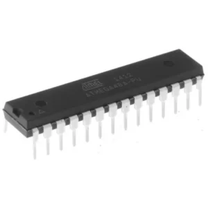
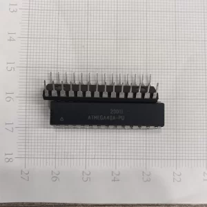
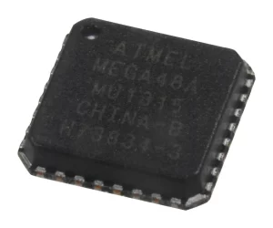
Read IC ATtiny48A Heximal refers to a controlled engineering service focused on accessing heximal and binary content stored inside a secured ATtiny48A microcontroller. As a compact AVR MCU, the ATtiny48A integrates on-chip flash, EEPROM, SRAM, timers, and communication peripherals within a small, cost-efficient chip. In production systems, its internal firmware, configuration data, and execution program are frequently locked, protected, or partially encrypted to safeguard intellectual property. When original source code or design files are unavailable, reading out the internal memory becomes critical for continuity and compliance.
The Stack is mainly used for storing temporary data, for storing local variables and for storing return addresses after interrupts and subroutine calls. The Stack Pointer Register always points to the top of the Stack. Note that the Stack is implemented as growing from higher memory locations to lower memory locations.
This implies that a Stack PUSH command decreases the Stack Pointer. The Stack Pointer points to the data SRAM Stack area where the Subroutine and Interrupt Stacks are located. This Stack space in the data SRAM must be defined by the program before any subroutine calls are executed or interrupts are enabled.
The Stack Pointer must be set to point above 0x0200. The initial value of the stack pointer is the last address of the internal SRAM. The Stack Pointer is decremented by one when data is pushed onto the Stack with the PUSH instruction, and it is decremented by three when the return address is pushed onto the Stack with subroutine call or interrupt.
The Stack Pointer is incremented by one when data is popped from the Stack with the POP instruction, and it is incremented by three when data is popped from the Stack with return from subroutine RET or return from interrupt RETI.
The AVR Stack Pointer is implemented as two 8-bit registers in the I/O space. The number of bits actually used is implementation dependent. Note that the data space in some implementations of the AVR architecture is so small that only SPL is needed.
In this case, the SPH Register will not be present. This section describes the general access timing concepts for instruction execution. The AVR CPU is driven by the CPU clock clkCPU, directly generated from the selected clock source for the chip. No internal clock division is used.
Figure 9 shows the parallel instruction fetches and instruction executions enabled by the Harvard architecture and the fast-access Register File concept. This is the basic pipelining concept to obtain up to 1 MIPS per MHz with the corresponding unique results for functions per cost, functions per clocks, and functions per power-unit.
The AVR provides several different interrupt sources. These interrupts and the separate Reset Vector each have a separate program vector in the program memory space. All interrupts are assigned individual enable bits which must be written logic one together with the Global Interrupt Enable bit in the Status Register in order to enable the interrupt.
Depending on the Program Counter value, interrupts may be automatically disabled when Boot Lock bits BLB02 or BLB12 are programmed. This feature improves software security. See the section “Memory Programming” on page 335 for details.
The lowest addresses in the program memory space are by default defined as the Reset and Interrupt Vectors. The complete list of vectors is shown in “Interrupts” on page 69. The list also determines the priority levels of the different interrupts. The lower the address the higher is the priority level.
RESET has the highest priority, and next is INT0 – the External Interrupt Request 0. The Interrupt Vectors can be moved to the start of the Boot Flash section by setting the IVSEL bit in the MCU Control Register (MCUCR).
In practical terms, Read IC ATtiny48A Heximal emphasizes disciplined reverse engineering rather than attempts to hack a device. The objective is to extract, open, and recover the internal contents of flash and EEPROM without compromising data integrity. Engineers assemble a validated dump and organize it into a consistent archive or file format suitable for analysis and reuse. Because security fuses are designed to prevent casual access, every step prioritizes accuracy and preservation, enabling a safe restore of operational knowledge from the microprocessor while avoiding destructive outcomes.
The ATtiny48A is widely deployed in consumer electronics, smart sensors, access control modules, lighting drivers, small appliances, and industrial auxiliary boards. Its low power consumption and flexible I/O make it ideal for embedded products that must operate reliably for years. Over time, manufacturers encounter discontinued components, undocumented revisions, or third-party systems requiring duplication. In these scenarios, Read IC ATtiny48A Heximal provides a practical path to maintain legacy platforms by consolidating firmware, calibration data, and runtime parameters into a dependable archive.
Breaking off protection on a secured ATtiny48A presents genuine challenges. Readout locks and internal safeguards increase the risk of data loss if mishandled, which is why detailed techniques are not disclosed. Nonetheless, the purpose is clear: preserve value. For clients, the benefits include reduced redevelopment costs, faster troubleshooting, reliable backups of binary and heximal assets, and the ability to replicate or migrate designs lawfully. By transforming inaccessible memory into actionable knowledge, Read IC ATtiny48A Heximal extends product lifecycles, minimizes downtime, and protects long-term investment in embedded systems.