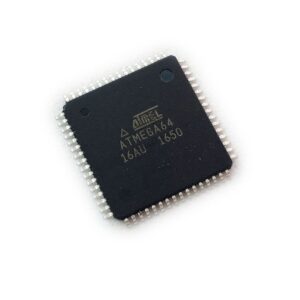
We can Read Chip ATMEGA64L Firmware, please view the Chip ATMEGA64L features for your reference:
Port C is an 8-bit bi-directional I/O port with internal pull-up resistors (selected for each bit). The Port C output buffers have symmetrical drive characteristics with both high sink and source capability. As inputs, Port C pins that are externally pulled low will source current if the pull-up resistors are activated.
Port D is an 8-bit bi-directional I/O port with internal pull-up resistors (selected for each bit). The Port D output buffers have symmetrical drive characteristics with both high sink and source capability. As inputs, Port D pins that are externally pulled low will source current if the pull-up resistors are activated.
The Port D pins are tri-stated when a reset condition becomes active, even if the clock is not running. Port E is an 8-bit bi-directional I/O port with internal pull-up resistors (selected for each bit). The Port E output buffers have symmetrical drive characteristics with both high sink and source capability.
As inputs, Port E pins that are externally pulled low will source current if the pull-up resistors are activated. The Port E pins are tri-stated when a reset condition becomes active, even if the clock is not running. Port F serves as the analog inputs to the A/D Converter.
Port F also serves as an 8-bit bi-directional I/O port, if the A/D Converter is not used. Port pins can provide internal pull-up resistors (selected for each bit) when readout atmega64 secured mcu eeprom and flash memory content. The Port F output buffers have symmetrical drive characteristics with both high sink and source capability.
As inputs, Port F pins that are externally pulled low will source current if the pull-up resistors are activated. The Port F pins are tri-stated when a reset condition becomes active, even if the clock is not running. If the JTAG interface is enabled, the pull-up resistors on pins PF7(TDI), PF5(TMS) and PF4(TCK) will be activated even if a reset occurs.
The TDO pin is tri-stated unless TAP states that shift out data are entered. Port G is a 5-bit bi-directional I/O port with internal pull-up resistors (selected for each bit). The Port G output buffers have symmetrical drive characteristics with both high sink and source capability. As inputs, Port G pins that are externally pulled low will source current if the pull-up resistors are activated. The Port G pins are tri-stated when a reset condition becomes active, even if the clock is not running. Port G also serves the functions of various special features.
In ATmega103 compatibility mode, these pins only serves as strobes signals to the external memory as well as input to the 32 kHz Oscillator, and the pins are initialized to PG0 = 1, PG1 = 1, and PG2 = 0 asynchronously when a reset condition becomes active, even if the clock is not running. PG3 and PG4 are Oscillator pins.