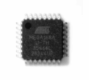
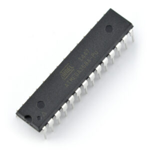
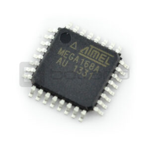
The phrase Read Chip ATmega168A Flash summarizes a sensitive but legitimate area of embedded systems work: extracting a binary or firmware archive from a microcontroller when that action is needed for lawful recovery, maintenance, or security research. The ATmega168A, part of the AVR family supported by Microchip, is a compact 8-bit microcontroller commonly chosen for its simplicity, low power, and flexible peripheral set. Its on-chip flash stores the device program, while EEPROM and SRAM hold persistent data and runtime state — all of which make the chip useful in a wide range of products.
Where ATmega168A appears
ATmega168A devices have historically been used in:
-
Hobbyist and educational platforms (earlier Arduino variants and small development boards)
-
Consumer peripherals and toys
-
Basic industrial controllers, sensor nodes, and data loggers
-
Home automation modules and low-cost IoT prototypes
In those roles the MCU often contains valuable intellectual property: compiled binary or heximal images of proprietary firmware, calibration data in EEPROM, or communication stacks. That is why manufacturers may mark devices as protected, locked, or otherwise configured to prevent casual readout or copying.
Read Chip ATmega168A Flash heximal needs to break the protection over mcu atmega168a and unlock microcontroller atmega168a flash and eeprom tamper resistance system by focus ion beam;
Most of the instructions operating on the Register File have direct access to all registers, and most of them are single cycle instructions. As shown in Figure 5-2, each register is also assigned a data memory address, mapping them directly into the first 32 locations of the user Data Space.
Although not being physically implemented as SRAM locations, this memory organization provides great flexibility in access of the registers, as the X-, Y- and Z-pointer registers can be set to index any register in the file. The registers R26..R31 have some added functions to their general purpose usage.
Why readout is sometimes necessary
There are legitimate circumstances to read chip ATmega168A flash: recovering lost firmware for legacy equipment, restoring devices after a corrupted update, performing authorized security audits, enabling interoperability for replacement modules, or archiving software for long-lived systems. For organizations maintaining fielded devices where source code has been misplaced or the original vendor no longer supports a product, a firmware dump may be essential to keep critical infrastructure running.
Keywords used in the ecosystem
Discussions around this topic commonly use terms such as crack / break /attack /decode /decapsulate /hack /decrypt /clone /copy /recover /replicate /duplicate /restore /reverse engineering. Nouns that frequently appear are firmware / source code / binary / heximal / EEPROM / flash / program / memory / file / data / archive / microcontroller / microprocessor / chip / MCU / dump. Adjectives important to the context include secured / protected / encrypted / locked. These words reflect both motivations and the technical/ethical boundaries of the activity.
These registers are 16-bit address pointers for indirect addressing of the data space. The three indirect address registers X, Y, and Z are defined as described in Figure 5-3. The Stack is mainly used for storing temporary data, for storing local variables and for storing return addresses after interrupts and subroutine calls.
The Stack Pointer Register always points to the top of the Stack. Note that the Stack is implemented as growing from higher memory locations to lower memory locations. This implies that a Stack PUSH command decreases the Stack Pointer.
The Stack Pointer points to the data SRAM Stack area where the Subroutine and Interrupt Stacks are located. This Stack space in the data SRAM must be defined by the program before any subroutine calls are executed or interrupts are enabled. The Stack Pointer must be set to point above 0x0100, preferably RAMEND.
The Stack Pointer is decremented by one when data is pushed onto the Stack with the PUSH instruction, and it is decremented by two when the return address is pushed onto the Stack with subroutine call or interrupt. The Stack Pointer is incremented by one when data is popped from the Stack with the POP instruction, and it is incremented by two when data is popped from the Stack with return from subroutine RET or return from interrupt RETI.
Practical and non-technical difficulties
Attempting to access a locked ATmega168A raises several non-procedural challenges. Logical protections—configured fuses or lock-bits—are intended to make standard interfaces refuse reads. Physical realities also matter: small packages, dense PCB layouts, and absence of exposed debug contacts complicate any invasive analysis and raise the risk of permanently destroying the device and its data. Interpreting a raw binary dump is another hurdle: compiled firmware lacks source-level symbols and often requires expert reverse engineering to reconstruct meaningful behavior. Finally, working on devices in regulated or safety-critical systems adds legal and safety constraints; incorrect restoration can introduce hazards.
Ethical and lawful framing
Because the vocabulary overlaps with illicit activity, it’s important to emphasize that any attempt to access protected firmware must be authorized and lawful. When the goal is legitimate — recovery, archival, compliance, or authorized security research — preferred routes include contacting the manufacturer, obtaining permission from the device owner, or hiring professional services that operate within legal frameworks.
The AVR Stack Pointer is implemented as two 8-bit registers in the I/O space. The number of bits actually used is implementation dependent. Note that the data space in some implementations of the AVR architecture is so small that only SPL is needed. In this case, the SPH Register will not be present.
This section describes the general access timing concepts for instruction execution. The AVR CPU is driven by the CPU clock clkCPU, directly generated from the selected clock source for the chip. No internal clock division is used.
Figure 5-4 shows the parallel instruction fetches and instruction executions enabled by the Harvard architecture and the fast-access Register File concept. This is the basic pipelining concept to obtain up to 1 MIPS per MHz with the corresponding unique results for functions per cost, functions per clocks, and functions per power-unit.
The AVR provides several different interrupt sources. These interrupts and the separate Reset Vector each have a separate program vector in the program memory space. All interrupts are assigned individual enable bits which must be written logic one together with the Global Interrupt Enable bit in the Status Register in order to enable the interrupt.
Depending on the Program Counter value, interrupts may be automatically disabled when Boot Lock bits BLB02 or BLB12 are programmed. This feature improves software security. See the section ”Memory Programming” on page 285 for details.
Read Chip ATmega168A Flash points to a complex intersection of technical capability, product lifecycle needs, and legal/ethical responsibility. The ATmega168A’s widespread deployment makes firmware recovery important in practice, but its protections, packaging, and the challenges of interpreting compiled program data mean that such work demands expertise, careful planning, and proper authorization — not shortcuts or irresponsible disclosure.