
The landscape of automotive and access-control security frequently relies on highly specialized silicon to authenticate users, manage wireless communications, and validate environmental variables. Among these unique components, the PIC16F639 stands out as an exceptional dual-die device that intelligently combines a standard 8-bit processing core with a highly specialized low-frequency (LF) analog front-end. This specific architecture is heavily deployed across the automotive manufacturing industry, serving as the trusted brain for passive keyless entry (PKE) systems, remote tire pressure monitoring networks, and secure RFID asset tracking logistics.
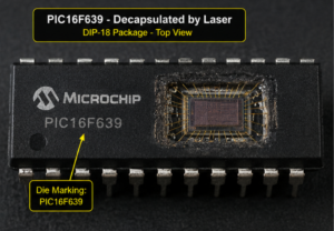
Because these commercial products dictate the physical security of high-value vehicles and restricted properties, the overarching engineering design strictly prioritizes keeping the internal operating logic completely hidden from external manipulation. When these specialized components inevitably fail out in the harsh conditions of the field, maintenance teams face the daunting, expensive task of interfacing with legacy hardware that was explicitly engineered to remain a permanent black box.
When the internal clock source is selected the TMR1H:TMR1L register pair will increment on multiples of FOSC as determined by the Timer1 prescaler. When the external clock source is selected, the Timer1 module may work as a timer or a counter. When counting, Timer1 is incremented on the rising edge of the external clock input T1CKI. In addition, the Counter mode clock can be synchronized to the microcontroller system clock or run asynchronously.
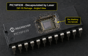
If an external clock oscillator is needed (and the microcontroller is using the INTOSC without CLKOUT), Timer1 can use the LP oscillator as a clock source. Timer1 has four prescaler options allowing 1, 2, 4 or 8 divisions of the clock input. The T1CKPS bits of the T1CON register control the prescale counter. The prescale counter is not directly readable or writable; however, the prescaler counter is cleared upon a write to TMR1H or TMR1L. A low-power 32.768 kHz crystal oscillator is built-in between pins OSC1 (input) and OSC2 (amplifier output). The oscillator is enabled by setting the T1OSCEN control bit of the T1CON register. The oscillator will continue to run during Sleep.
The Timer1 oscillator is shared with the system LP oscillator. Thus, Timer1 can use this mode only when the primary system clock is derived from the internal oscillator or when the oscillator is in the LP mode. The user must provide a software time delay to ensure proper oscillator start-up.
TRISA5 and TRISA4 bits are set when the Timer1 oscillator is enabled. RA5 and RA4 bits read as ‘0’ and TRISA5 and TRISA4 bits read as ‘1’. If control bit T1SYNC of the T1CON register is set, the external clock input is not synchronized. The timer increments asynchronously to the internal phase clocks. If external clock source is selected then the timer will continue to run during Sleep and can generate an interrupt on overflow, which will wake-up the processor. However, special precautions in software are needed to read/write the timer (see Section 6.5.1 “Reading and Writing Timer1 in Asynchronous Counter Mode”).
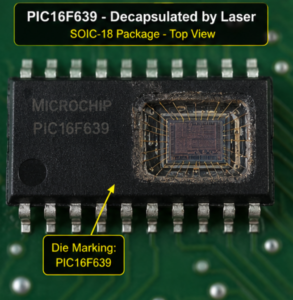
Overcoming the formidable defensive barriers of a secured and locked chip requires an intimate, microscopic understanding of its physical silicon topography. The primary difficulty when attempting to bypass these defenses is that the inner microprocessor actively guards its integrated memory against unauthorized access via permanently blown hardware fuses. If a technician wants to bypass a protected MCU, they cannot simply ping the component through standard diagnostic interfaces. Instead, sophisticated methods often involve physically decapping the semiconductor package to expose the delicate surface silicon structures, navigating past intricate anti-tamper meshes that physically shield the volatile flash storage and the eeprom cells. If an invasive chemical or electrical probe triggers a low-level alarm state during this highly sensitive physical procedure, the encrypted matrix will instantly initiate a self-erase sequence, permanently destroying the exact digital assets you are trying to secure.
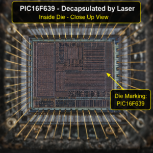
When an organization absolutely needs to hack or creatively open this rigid hardware architecture, the ultimate goal is to safely extract and recover the foundational machine instructions intact. Through highly precise reverse engineering workflows, laboratory engineers can initiate a specialized read sequence to safely dump the raw binary or heximal file directly from the exposed logic gates. This newly liberated data archive contains the precise program necessary to exactly replicate the failing system’s behavior, acting as a functional bridge to restore daily operations without ever needing access to the original vendor’s proprietary source code. Once the native firmware is successfully isolated and verified into a stable, uncorrupted archive, it fundamentally transforms from an inaccessible hardware mystery into a highly legible, infinitely manageable digital asset.
Why do industrial and commercial entities undertake such rigorous, technically demanding procedures? The harsh reality of global infrastructure is that legacy operating systems and their physical host boards frequently outlast the original component manufacturers. When a commercial transport fleet or a facility’s localized access control grid relies on obsolete electronics that are no longer supported by the OEM, a single blown circuit can mandate a multimillion-dollar, ground-up system replacement. By executing these advanced retrieval methodologies, we provide our clients with total, uncompromising technological independence. Securing the functional logic grants businesses the immediate leverage to clone end-of-life parts, patch latent software vulnerabilities, and sustain critical operations indefinitely, ensuring that their long-term capital investments are never held hostage by the failure of a single microcontroller.