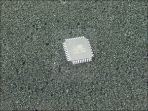
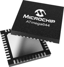
As embedded systems age and technical support evolves, organizations frequently encounter situations requiring access to firmware stored within legacy microcontrollers. Our professional service specializes in the secure extraction and analysis of program code from advanced AVR chips, including the ATmega644. This microcontroller, widely implemented in industrial controls, medical devices, and communication equipment, often contains proprietary firmware protected by hardware security features. Our methodology provides engineers with legitimate access to this essential software for system maintenance, compatibility verification, and technological migration projects.
Navigating Security Protocols in Advanced Microcontrollers
The ATmega644 incorporates sophisticated security architectures designed to protect intellectual property within its memory systems. These protective measures typically include locked programming interfaces, encrypted memory segments, and verification routines that prevent unauthorized reading of firmware content. Our engineers employ specialized hardware interfaces and signal protocol analysis to establish controlled communication with the chip’s internal systems. This initial connection allows us to map the memory architecture, identifying both flash program segments and EEPROM data regions while preserving the physical integrity of the microcontroller. This careful approach enables us to extract the complete binary content without triggering permanent security locks that could render the chip inoperable.
Our extraction process involves systematic reverse engineering of the microcontroller’s security implementation. By analyzing how the ATmega644 implements its protective measures, we develop customized protocols to access the secured memory regions. This careful examination allows for complete recovery of the firmware in its original binary format, creating an exact digital replica of the program stored within the chip. The resulting hexadecimal file serves as a complete archive of the original firmware, containing both executable instructions and critical configuration data. Following extraction, we process this raw binary information through reconstruction algorithms that restore the logical organization of the software, transforming the extracted data into functional files suitable for analysis or redeployment.
Applications and Benefits of Professional Firmware Access
This technical capability serves multiple legitimate purposes across various industries. Manufacturers utilize our extraction services to maintain legacy systems when original source code has been lost or when documentation is incomplete. Research institutions benefit from firmware analysis for compatibility studies and system interoperability testing. Technical teams recovering from hardware failures gain access to backup firmware when conventional recovery methods prove ineffective. Unlike destructive or questionable approaches, our methodology prioritizes the integrity of both the physical microcontroller and the extracted software archive, ensuring that clients receive functional firmware suitable for their engineering requirements.
The process yields more than just extracted code—it creates a comprehensive technical foundation for future development. The resulting files provide complete documentation of the firmware’s architecture, including memory allocation, interrupt handling, and hardware interface protocols. This detailed recovery enables engineers to understand legacy system operation, develop compatible hardware interfaces, and create updated versions of essential firmware. For organizations facing technological obsolescence or compatibility challenges, this professional extraction service bridges the gap between legacy implementations and modern development requirements.
Conclusion: Value of Systematic Firmware Recovery
Professional extraction of microcontroller firmware represents an essential service in today’s complex technological landscape. Our specialized approach to accessing secured chips like the ATmega644 transforms protected, inaccessible systems into analyzable software archives. By employing precise methodologies that respect both hardware integrity and intellectual property considerations, we provide engineering teams with the technical resources needed to maintain, understand, and evolve critical embedded systems. This service ensures valuable firmware remains accessible for legitimate engineering purposes, supporting continued innovation and system reliability across multiple industries.
There are several issues to consider when trying to minimize the power consumption in an AVR controlled system. In general, sleep modes should be used as much as possible, and the sleep mode should be selected so that as few as possible of the device’s functions are operating.
All functions not needed should be disabled. In particular, the following modules may need special consideration when trying to achieve the lowest possible power consumption.
If enabled, the ADC will be enabled in all sleep modes. To save power, the ADC should be disabled before entering any sleep mode. When the ADC is turned off and on again, the next conversion will be an extended conversion. Refer to “Analog to Digital Converter” on page 274 for details on ADC operation.
When entering Idle mode, the Analog Comparator should be disabled if not used. When entering ADC Noise Reduction mode, the Analog Comparator should be disabled. In other sleep modes, the Analog Comparator is automatically disabled.
However, if the Analog Comparator is set up to use the Internal Voltage Reference as input, the Analog Comparator should be disabled in all sleep modes. Otherwise, the Internal Voltage Reference will be enabled, independent of sleep mode. Refer to “Analog Comparator” on page 271 for details on how to configure the Analog Comparator.
If the Brown-out Detector is not needed by the application, this module should be turned off. If the Brown-out Detector is enabled by the BODLEVEL Fuses, it will be enabled in all sleep modes, and hence, always consume power. In the deeper sleep modes, this will contribute significantly to the total current consumption.
Refer to “Brown-out Detection” on page 59 for details on how to configure the Brown-out Detector.
The Internal Voltage Reference will be enabled when needed by the Brown-out Detection, the Analog Comparator or the ADC. If these modules are disabled as described in the sections above, the internal voltage reference will be disabled and it will not be consuming power.
When turned on again, the user must allow the reference to start up before the output is used. If the reference is kept on in sleep mode, the output can be used immediately. Refer to “Internal Voltage Reference” on page 62 for details on the start-up time.
If the Watchdog Timer is not needed in the application, the module should be turned off. If the Watchdog Timer is enabled, it will be enabled in all sleep modes, and hence, always consume power. In the deeper sleep modes, this will contribute significantly to the total current consumption. Refer to “Interrupts” on page 69 for details on how to configure the Watchdog Timer.
When entering a sleep mode, all port pins should be configured to use minimum power. The most important is then to ensure that no pins drive resistive loads. In sleep modes where both the I/O clock (clkI/O) and the ADC clock (clkADC) are stopped, the input buffers of the device will be disabled.
This ensures that no power is consumed by the input logic when not needed. In some cases, the input logic is needed for detecting wake-up conditions, and it will then be enabled. Refer to the section “Digital Input Enable and Sleep Modes” on page 85 for details on which pins are enabled.
If the input buffer is enabled and the input signal is left floating or have an analog signal level close to VCC/2, the input buffer will use excessive power. For analog input pins, the digital input buffer should be disabled at all times. An analog signal level close to VCC/2 on an input pin can cause significant current even in active mode.
Digital input buffers can be disabled by writing to the Digital Input Disable Registers (DIDR2, DIDR1 and DIDR0). Refer to “Digital Input Disable Register 2 – DIDR2” on page 293, “Digital Input Disable Register 1 – DIDR1” on page 273 and “Digital Input Disable Register 0 – DIDR0” on page 293 for details.