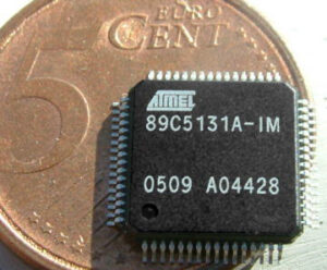
Extract MCU AT89C5131 Code from its secured memory which include the flash and eeprom, after unlock microcontroller protective system and locate the fuse bit, focus ion beam can cut it off for IC cloning;
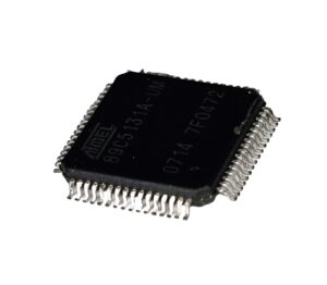
Restoring flash binary from a locked MCU AT89C5131 is a technically demanding task that draws the interest of security researchers, hardware engineers, and reverse engineers alike. The AT89C5131, a member of Atmel’s 8051-based microcontroller family, features robust protection mechanisms that make firmware recovery particularly difficult. Combined with its sibling AT89C5130A, this MCU line is well-known for its secured architecture and advanced USB capabilities.
Key Features of the AT89C5131 and AT89C5130A
The AT89C5131 and AT89C5130A microcontrollers are 8-bit MCUs built on the 8051 architecture, with notable enhancements including:
USB 2.0 full-speed device support
64 KB of flash memory
2304 bytes of on-chip RAM
Integrated bootloader
Flexible SPI, UART, and I2C interfaces
These features make the AT89C5131 ideal for USB peripherals and embedded systems requiring secure communication and data handling. However, the same features that make it powerful also increase the difficulty of performing flash binary restoration.
These security bits protect the code access through the parallel programming interface. They are set by default to level 4. The code access through the ISP is still possible and is controlled by the “software security bits” which are stored in the extra Flash memory accessed by the ISP firmware when Extract ic at89s51 firmware.
To load a new application with the parallel programmer, a chip erase must be done first. This will set the HSB in its inactive state and will erase the Flash memory. The part reference can always be read using Flash parallel programming modes.
The default value of the HSB provides parts ready to be programmed with ISP:
BLJB: Cleared to force ISP operation.
X2: Set to force X1 mode (Standard Mode)
OSCON1-0: Set to start with 32 MHz oscillator configuration value.
LB2-0: Security level four to protect the code from a parallel access with maximum security.
Software Registers
Several registers are used, in factory and by parallel programmers, to make copies of hardware registers contents. These values are used by Atmel ISP (see Section “In-System Programming (ISP)”). These registers are in the “Extra Flash Memory” part of the Flash memory. This block is also called ”XAF” or eXtra Array Flash. They are accessed in the following ways:
Commands issued by the parallel memory programmer.
Commands issued by the ISP software.
Calls of API issued by the application software.
Several software registers are described in Table 39.
In the AT89C5131, the lowest 16K or 32K of the 64 Kbyte program memory address space is filled by internal Flash. When the EA is pin high, the processor fetches instructions from internal program Flash. Bus expansion for accessing program memory from 16K or 32K upward is automatic since external instruction fetches occur automatically when the program counter exceeds 3FFFh (16K) or 7FFFh (32K).
If the EA pin is tied low, all program memory fetches are from external memory. If all storage is on chip, then byte location 3FFFh (16K) or 7FFFh (32K) should be left vacant to prevent and undesired pre-fetch from external program memory address 4000h (16K) or 8000h (32K).
The 1-Kbyte on-chip EEPROM memory block is located at addresses 0000h to 03FFh of the ERAM memory space and is selected by setting control bits in the EECON register before Extract MCU. A read in the EEPROM memory is done with a MOVX instruction. A physical write in the EEPROM memory is done in two steps: write data in the column latches and transfer of all data latches into an EEPROM memory row (programming) after Extract MCU AT89LS51 Firmware.
The number of data written on the page may vary from 1 to 128 bytes (the page size). When programming, only the data written in the column latch is programmed and a ninth bit is used to obtain this feature. This provides the capability to program the whole memory by bytes, by page or by a number of bytes in a page. Indeed, each ninth bit is set when the writing the corresponding byte in a row and all these ninth bits are reset after the writing of the complete EEPROM row..