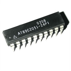
Extract MCU AT89C2051 Code is a process to dump the firmware in the format of heximal out from the flash and eeprom memory, normally protection of microcontroller will be unlocked for this reason;
Fuse Protection Mechanism: The microcontroller implements locked fuse bits that block access to the program memory, making code recovery or replication extremely difficult.
Decapsulation Attack: Physically removing the protective layers of the chip can provide direct access to internal circuits, but it requires specialized equipment and expertise.
EEPROM Dumping and Flash Extraction: Even if the binary data is extracted, it may be encrypted, preventing successful cloning or duplication.
Glitch and Fault Injection Attacks: These techniques involve voltage manipulation to bypass secured memory areas, but their success depends on the microcontroller’s security strength.
Reverse Engineering: If partial firmware archives or program files are available, advanced decoding techniques can help reconstruct the original source code.
Ethical and Legal Considerations
Attempting to extract or decrypt AT89C2051 firmware without authorization raises legal and ethical issues. Secured microcontrollers are designed to prevent unauthorized duplication or hacking. If you need access to locked program data, always follow legal guidelines and obtain proper permissions.
In conclusion, extracting MCU AT89C2051 code is a highly technical challenge due to its locked flash memory and fuse protection. While methods such as decapsulation, fault injection, and EEPROM dumping exist, successfully decrypting and copying the microcontroller’s secured firmware remains an advanced and legally sensitive task.
To Program and Verify the Array:
- Apply data for Code byte at location 000H to P1.0 to P1.7.
- Raise RST to 12V to enable programming.
- Pulse P3.2 once to program a byte in the PEROM array or the lock bits. The byte-write cycle is self-timed and typically takes 1.2 ms.
- To verify the programmed data, lower RST from 12V to logic “H” level and set pins P3.3 to P3.7 to the appropriate levels. Output data can be read at the port P1 pins.
- To program a byte at the next address location, pulse XTAL1 pin once to advance the internal address counter. Apply new data to the port P1 pins.
- Repeat steps 6 through 8, changing data and advancing the address counter for the entire 2K bytes array or until the end of the object file is reached.
- Power-off sequence: set XTAL1 to “L” set RST to “L”
Turn VCC power off
Data Polling: The AT89C2051 features Data Polling to indicate the end of a write cycle. During a write cycle, an attempted read of the last byte written will result in the complement of the written data on P1.7. Once the write cycle has been completed, true data is valid on all outputs, and the next cycle may begin. Data Polling may begin any time after a write cycle has been initiated before Extract Microcontroller at89lv52 code.
Ready/Busy: The Progress of byte programming can also be monitored by the RDY/BSY output signal. Pin P3.1 is pulled low after P3.2 goes High during programming to indicate BUSY. P3.1 is pulled High again when programming is done to indicate READY.
Program Verify: If lock bits LB1 and LB2 have not been programmed code data can be read back via the data lines for verification:
- Reset the internal address counter to 000H by bringing RST from “L” to “H”.
- Apply the appropriate control signals for Read Code data and read the output data at the port P1 pins.
- Pulse pin XTAL1 once to advance the internal address counter.
- Read the next code data byte at the port P1 pins.
- Repeat steps 3 and 4 until the entire array is read.
The lock bits cannot be verified directly. Verification of the lock bits is achieved by observing that their features are enabled.
Chip Erase: The entire PEROM array (2K bytes) and the two Lock Bits are erased electrically by using the proper combination of control signals and by holding P3.2 low for 10 ms. The code array is written with all “1”s in the Chip Erase operation and must be executed before any non-blank memory byte can be re-programmed.
Reading the Signature Bytes: The signature bytes are read by the same procedure as a normal verification of locations 000H, 001H, and 002H, except that P3.5 and P3.7 must be pulled to a logic low. The values returned are as follows. (000H) = 1EH indicates manufactured by Atmel (001H) = 21H indicates 89C2051 Every code byte in the Flash array can be written and the entire array can be erased by using the appropriate combination of control signals. The write operation cycle is self-timed and once initiated, will automatically time itself to completion before Extract Microcontroller at89c1051 code.
Most major worldwide programming vendors offer support for the Atmel AT89 microcontroller series. Please contact your local programming vendor for the appropriate software revision. In the power-down mode the oscillator is stopped, and the instruction that invokes power-down is the last instruction executed.
The on-chip RAM and Special Function Registers retain their values until the power-down mode is terminated. The only exit from power-down is a hardware reset. Reset redefines the SFRs but does not change the on-chip RAM. The reset should not be activated before VCC is restored to its normal operating level and must be held active long enough to allow the oscillator to restart and stabilize.
The P1.0 and P1.1 should be set to “0” if no external pull-ups are used, or set to “1” if external pull-ups are used.