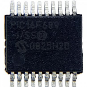
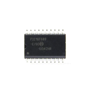
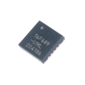
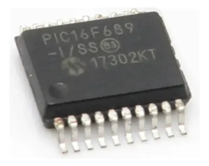
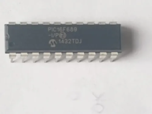
In the rapidly evolving world of embedded hardware electronics, preserving operational continuity often requires specialized engineering interventions. A primary challenge faced by maintenance teams today is the need to Extract IC PIC16F689 Code from legacy systems where the original documentation has been lost. The PIC16F689 itself is a highly versatile microcontroller featuring a robust 20-pin architecture, an integrated analog-to-digital converter (ADC), and precise internal oscillators. Because of its cost-effective footprint and reliability, this specific MCU is widely deployed across automated industrial manufacturing lines, commercial security alarm systems, and automotive climate control modules. However, when these systems require critical updates or hardware migration, engineers must find ethical ways to open, hack, or reverse engineering the system to retrieve the underlying assets. When dealing with an obsolete or end-of-life chip, extracting the internal instructions becomes the only viable strategy to prevent catastrophic system downtime.
The HFINTOSC is factory calibrated but can be adjusted in software by writing to the OSCTUNE register (Register 3-2). The default value of the OSCTUNE register is ‘0’. The value is a 5-bit two’s complement number.
When the OSCTUNE register is modified, the HFINTOSC frequency will begin shifting to the new frequency. Code execution continues during this shift. There is no indication that the shift has occurred.
OSCTUNE does not affect the LFINTOSC frequency. Operation of features that depend on the LFINTOSC clock source frequency, such as the Power-up Timer (PWRT), Watchdog Timer (WDT), Fail-Safe Clock Monitor (FSCM) and peripherals, are not affected by the change in frequency.
The Low-Frequency Internal Oscillator (LFINTOSC) is an uncalibrated 31 kHz internal clock source. The output of the LFINTOSC connects to a postscaler and multiplexer (see Figure 3-1). Select 31 kHz, via software, using the IRCF<2:0> bits of the OSCCON register.
See Section 3.5.4 “Frequency Select Bits (IRCF)” for more information. The LFINTOSC is also the frequency for the Power-up Timer (PWRT), Watchdog Timer (WDT) and Fail-Safe Clock Monitor (FSCM).
The LFINTOSC is enabled by selecting 31 kHz (IRCF<2:0> bits of the OSCCON register = 000) as the system clock source (SCS bit of the OSCCON register = 1), or when any of the following are enabled;
- Two-Speed Start-up IESO bit of the Configuration Word register = 1 and IRCF<2:0> bits of the OSCCON register = 000
- Power-up Timer (PWRT)
- Watchdog Timer (WDT)
· Fail-Safe Clock Monitor (FSCM)
The LF Internal Oscillator (LTS) bit of the OSCCON register indicates whether the LFINTOSC is stable or not. The output of the 8 MHz HFINTOSC and 31 kHz LFINTOSC connects to a postscaler and multiplexer (see Figure 3-1). The Internal Oscillator Frequency Select bits IRCF<2:0> of the OSCCON register select the frequency output of the internal oscillators. One of eight frequencies can be selected via software.
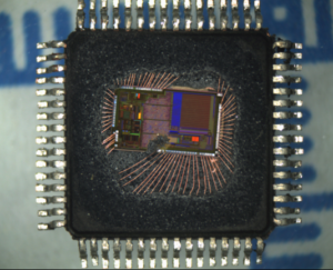
The technical process of managing a secured, protected, or locked semiconductor requires deep familiarity with how internal memory arrays hold proprietary assets. When specialists attempt to extract, recover, or restore a functional program from a hardened device, they must isolate the raw binary or heximal file hidden within the silicon layers. This highly concentrated operation aims to safely dump the flash memory and the integrated eeprom space, which together form the operational data archive of the machinery. Successfully executing this extraction allows teams to reconstruct the firmware and approximate the original source code layout without destroying the physical component. Because these integrated circuits utilize hardware-level fuse bits to block unauthorized programming access, bypassing these barriers requires specialized logic analyzers and precise environmental manipulation to force the microprocessor to yield its data without triggering a self-erase protective sequence.
Overcoming these internal defense mechanisms introduces a steep learning curve and several distinct technical hurdles. Modern MCU designs utilize active security meshes, clock-frequency monitoring, and voltage tamper detection routines to keep the inner flash space permanently encrypted against external reading tools. If the extraction tool applies incorrect voltage tolerances during a read attempt, the microprocessor will instantly lock down or wipe its internal eeprom data permanently. Why do businesses choose to take these calculated risks to open up a protected architecture? The necessity arises when original equipment manufacturers (OEMs) go out of business or stop supporting older hardware revisions. Without a way to safely extract and recover the functional software layer, an entire industrial assembly line or specialized medical device could become completely unserviceable due to a single faulty silicon component.
Ultimately, securing a clean heximal or binary dump from a legacy circuit delivers immense strategic and financial benefits to our clients. By utilizing highly controlled hardware reverse engineering methodologies, asset managers can actively safeguard their infrastructure against forced obsolescence and costly vendor lock-in. Having an accessible, verified file archive of the device firmware allows engineering teams to easily patch software vulnerabilities, clone failing components onto newer hardware, and ensure long-term operational compliance. This protective approach transforms an inaccessible, locked hardware asset back into an open, fully documented platform—drastically reducing maintenance overhead, mitigating supply chain vulnerabilities, and ensuring continuous business operations for years to come.