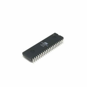
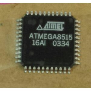
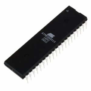
The demand to extract IC ATMEGA8515 program arises in many cases, especially when dealing with secured or locked embedded systems. The ATMEGA8515, designed by Atmel (now Microchip), is an 8-bit microcontroller based on the AVR RISC architecture. It features 8KB of in-system programmable flash memory, 512B of EEPROM, and 512B of SRAM. With its high performance and efficient instruction set, this MCU has been widely deployed in industrial controllers, instrumentation devices, consumer electronics, robotics, and communication modules. Its flexible I/O lines, timers, UART, SPI, and external memory interface make it a versatile solution for embedded applications.
When a project requires recovering firmware from a secured device, the challenges are significant. The ATMEGA8515 implements lock bits that prevent reading of binary or heximal content from the internal flash. Once these security fuses are set, any standard programmer or debug tool cannot access the program file, making direct copying, cloning, or dumping impossible.
The AVR core combines a rich instruction set with 32 general purpose working registers. All the 32 registers are directly connected to the Arithmetic Logic Unit (ALU), allowing two independent registers to be accessed in one single instruction executed in one clock cycle.
The resulting architecture is more code efficient while achieving throughputs up to ten times faster than conventional CISC microcontrollers.
The ATmega8515 provides the following features: 8K bytes of In-System Programmable Flash with Read-While-Write capabilities, 512 bytes EEPROM, 512 bytes SRAM, an External memory interface, 35 general purpose I/O lines, 32 general purpose working registers, two flexible Timer/Counters with compare modes, Internal and External interrupts, a Serial Programmable USART, a programmable Watchdog Timer with internal Oscillator, a SPI serial port, and three software selectable power saving modes.
To overcome these restrictions, engineers use highly advanced reverse engineering and chip attack methodologies. These may include:
-
Decapsulation – Physically removing the plastic packaging of the chip to expose the silicon die. Once the die is visible, high-powered microscopes and laser-based techniques may be used to analyze and manipulate security circuits.
-
Fault injection attacks – Using voltage glitches, clock manipulation, or electromagnetic pulses to force the MCU into an unprotected state where the firmware can be read.
-
Side-channel analysis – Monitoring power consumption or electromagnetic emissions to decode the sequence of instructions, ultimately leading to reconstruction of the data.
-
Microprobing – Directly probing internal buses on the die to extract binary archives from the memory.
These techniques are resource-intensive and demand expert knowledge in hardware security. Each method carries risks: damaging the chip, corrupting the program, or requiring multiple attempts before a successful dump can be achieved.
The Idle mode stops the CPU while allowing the SRAM, Timer/Counters, SPI port, and Interrupt system to continue functioning. The Power-down mode saves the Register contents but freezes the Oscillator, disabling all other chip functions until the next interrupt or hardware reset. In Standby mode, the crystal/resonator Oscillator is running while the rest of the device is sleeping. This allows very fast start-up combined with low-power consumption.
The device is manufactured using Atmel’s high density nonvolatile memory technology. The On-chip ISP Flash allows the Program memory to be reprogrammed In-System through an SPI serial interface, by a conventional nonvolatile memory programmer, or by an On-chip Boot program running on the AVR core.
The boot program can use any interface to download the application program in the Application Flash memory. Software in the Boot Flash section will continue to run while the Application Flash section is updated after extracting atmega8515l microcontroller flash memory firmware, providing true Read-While-Write operation.
By combining an 8-bit RISC CPU with In-System Self-programmable Flash on a monolithic chip, the Atmel ATmega8515 is a powerful microcontroller that provides a highly flexible and cost effective solution to many embedded control applications.
The ATmega8515 is supported with a full suite of program and system development tools including: C Compilers, Macro assemblers, Program debugger/simulators, In-circuit Emulators, and Evaluation kits. Typical values contained in this datasheet are based on simulations and characterization of other AVR microcontrollers manufactured on the same process technology. Min and Max values will be available after the device is characterized.
The motivation to break or hack into a secured ATMEGA8515 often comes from the need to restore lost intellectual property, recover legacy source code for product maintenance, or replicate an old design where the original development files no longer exist. In many industries such as automotive controllers, industrial PLCs, and robotics systems, these MCUs are embedded deep into machines, and the ability to duplicate or copy the original firmware ensures continuity of production and long-term support.
However, the protected and encrypted design of the ATMEGA8515 makes it resistant to simple attack attempts. The process to extract its program file is complex, requiring sophisticated lab-grade equipment and specialized expertise. Unlike ordinary microprocessors, this device incorporates multiple layers of hardware security, making reverse engineering a delicate and challenging operation.
In conclusion, the task to extract IC ATMEGA8515 program highlights the cutting edge of firmware recovery and reverse engineering. Through advanced cracking techniques, engineers can recover, replicate, or restore essential data archives from this secured microcontroller, ensuring that critical embedded systems continue to function even when the original development environment is lost.