Extract IC ATmega644A Code refers to the specialized process of retrieving binary or heximal files from a secured and locked ATmega644A microcontroller when conventional access methods are blocked. In many embedded systems, the firmware and source code stored inside the MCU represent the core operational logic of a product. When protection bits are enabled, the flash and EEPROM memory become inaccessible through standard programming interfaces, preventing engineers from reading or copying the internal program data. Through structured reverse engineering practices, it becomes possible to extract, recover, and restore valuable memory archives from a protected chip without disclosing proprietary techniques. This service is often essential when original development files are lost or when long-term product maintenance depends on access to the internal binary dump.
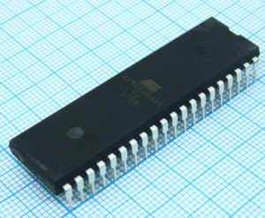
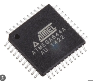
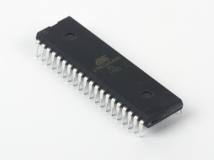
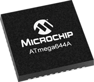
The ATmega644A is an 8-bit AVR microcontroller designed for reliability and versatility in medium-complexity embedded applications. It offers substantial flash memory capacity, EEPROM for non-volatile data storage, and SRAM for runtime operations. With multiple communication peripherals such as SPI, USART, and TWI, along with timers, PWM channels, analog comparators, and flexible GPIO lines, this MCU supports a wide range of industrial and commercial deployments. The ATmega644A microprocessor is commonly integrated into industrial controllers, energy management devices, smart instrumentation, access control systems, agricultural automation equipment, and specialized consumer electronics. In these applications, the firmware stored inside the chip governs communication protocols, sensor processing algorithms, motor control logic, and safety routines. The internal memory structure, including flash program space and EEPROM data areas, effectively acts as a digital archive of the product’s intelligence.
Extract IC ATmega644A Code needs to unlock mcu atmega644a protective system and locate the fuse bit through reverse engineering microcontroller atmega644a internal structure;
If the On-chip debug system is enabled by the OCDEN Fuse and the chip enters sleep mode, the main clock source is enabled, and hence, always consumes power. In the deeper sleep modes, this will contribute significantly to the total current consumption.
There are three alternative ways to disable the OCD system: Disable the OCDEN Fuse. Disable the JTAGEN Fuse. Write one to the JTD bit in MCUCR.
During reset, all I/O Registers are set to their initial values, and the program starts execution from the Reset Vector. The instruction placed at the Reset Vector must be a JMP – Absolute Jump – instruction to the reset handling routine.
If the program never enables an interrupt source, the Interrupt Vectors are not used, and regular program code can be placed at these locations. This is also the case if the Reset Vector is in the Application section while the Interrupt Vectors are in the Boot section or vice versa.
The circuit diagram in Figure 25 shows the reset logic. Table 23 defines the electrical parameters of the reset circuitry. The I/O ports of the AVR are immediately reset to their initial state when a reset source goes active. This does not require any clock source to be running.
After all reset sources have gone inactive, a delay counter is invoked, stretching the internal reset. This allows the power to reach a stable level before normal operation starts. The time-out period of the delay counter is defined by the user through the SUT and CKSEL Fuses. The different selections for the delay period are presented in “Clock Sources”.
The ATmega644 has five sources of reset: Power-on Reset. The MCU is reset when the supply voltage is below the Power-on Reset threshold (VPOT). External Reset. The MCU is reset when a low level is present on the RESET pin for longer than the minimum pulse length.
Watchdog Reset. The MCU is reset when the Watchdog Timer period expires and the Watchdog is enabled. Brown-out Reset. The MCU is reset when the supply voltage VCC is below the Brown-out Reset threshold (VBOT) and the Brown-out Detector is enabled.
JTAG AVR Reset. The MCU is reset as long as there is a logic one in the Reset Register, one of the scan chains of the JTAG system. Refer to the section “IEEE 1149.1 (JTAG) Boundary-scan” on page 301 for details.
A Power-on Reset (POR) pulse is generated by an On-chip detection circuit. The detection level is defined in Table 23. The POR is activated whenever VCC is below the detection level. The POR circuit can be used to trigger the start-up Reset, as well as to detect a failure in supply voltage.
A Power-on Reset (POR) circuit ensures that the device is reset from Power-on. Reaching the Power-on Reset threshold voltage invokes the delay counter, which determines how long the device is kept in RESET after VCC rise. The RESET signal is activated again, without any delay, when VCC decreases below the detection level.
An External Reset is generated by a low level on the RESET pin. Reset pulses longer than the minimum pulse width (see Table 23) will generate a reset, even if the clock is not running. Shorter pulses are not guaranteed to generate a reset. When the applied signal reaches the Reset Threshold Voltage – VRST – on its positive edge, the delay counter starts the MCU after the Time-out period – tTOUT – has expired.
ATmega644 has an On-chip Brown-out Detection (BOD) circuit for monitoring the VCC level during operation by comparing it to a fixed trigger level. The trigger level for the BOD can be selected by the BODLEVEL Fuses. The trigger level has a hysteresis to ensure spike free Brown-out Detection. The hysteresis on the detection level should be interpreted as VBOT+ = VBOT + VHYST/2 and VBOT- = VBOT – VHYST/2.
Extract IC ATmega644A Code projects frequently involve scenarios where clients need to hack access to their own secured hardware in order to recover lost firmware or restore production continuity. When a microcontroller is protected, encrypted, or fuse-locked, direct attempts to open the memory interface typically result in blocked readout or automatic erase functions. Engineers may encounter encrypted segments, locked bootloader regions, checksum verification routines, and strict read-protection mechanisms embedded at the silicon level. Reverse engineering a secured ATmega644A chip therefore demands in-depth knowledge of AVR architecture, memory mapping, and protection logic. The objective is not simply to dump data, but to carefully extract consistent binary or heximal files from flash and EEPROM without corrupting the stored program or damaging the MCU itself. Each step must be executed with precision to ensure that recovered firmware remains complete and usable.
The ability to extract and restore firmware from a locked ATmega644A microcontroller delivers significant operational and commercial value. By recovering source code structures from binary data, organizations can resume halted production lines, repair legacy systems, and migrate designs to updated hardware platforms. Access to a clean firmware archive also supports troubleshooting, product upgrades, and compliance verification. Instead of redesigning an entire system due to inaccessible memory, clients can rebuild their development environment using restored program files and validated data dumps. Ultimately, Extract IC ATmega644A Code services transform a protected and inaccessible chip into a recoverable digital asset, preserving intellectual property, extending product lifecycles, and minimizing redevelopment costs for businesses operating in competitive technology sectors.