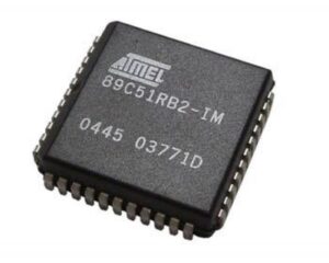
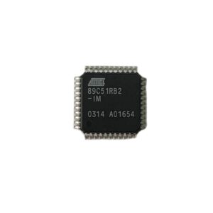
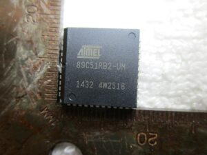
The ability to recover MCU AT89C51RB2 code from a secured or locked microcontroller represents a sophisticated blend of hardware forensics and embedded system intelligence. The AT89C51RB2, a high-performance 8051-based microcontroller from Atmel, is equipped with 16KB of in-system programmable flash, expanded EEPROM, and robust firmware security mechanisms. It is widely used in embedded control systems, industrial applications, and automotive platforms.
However, once the device’s security lock bits are activated, all standard methods of accessing internal memory are blocked. This means the embedded binary, source code, or heximal program becomes inaccessible through typical programming interfaces. To recover or dump the internal data, one must engage in deliberate, technically intensive operations often categorized under reverse engineering.
The process to crack, clone, or decrypt a protected AT89C51RB2 chip involves several possible approaches:
-
Decapsulation of the chip is the first physical step, exposing the silicon die by chemically removing the protective casing. This enables visual or electrical probing at the transistor level.
-
Microprobing techniques then allow attackers to read out memory cell values directly, bypassing standard access controls.
-
Fault injection using voltage or clock glitches may momentarily disable security logic, creating windows of vulnerability to copy or dump the archive.
-
Code analysis and firmware pattern recognition can also aid in reconstructing replicated program data from partial dumps or known behaviors.
The AT89C51RB2 distinguishes itself from other MCUs with an embedded bootloader and enhanced I/O features, as well as multiple security modes. These characteristics not only increase its usefulness but also amplify the difficulty of a successful attack. For example, protected code blocks cannot be accessed via standard ISP commands, and the encrypted flash segments prevent direct interpretation even when memory access is achieved.
Moreover, each failed hack attempt may trigger lockout mechanisms, making the chip unusable and erasing the firmware permanently. Therefore, a successful recovery process must be planned meticulously, using a combination of electrical engineering, chip analysis, and embedded software expertise.
To recover MCU AT89C51RB2 code is not merely a matter of bypassing protections — it is a detailed, high-stakes operation. When done successfully, the outcome is a complete binary file, ready for replication, duplication, or restoration — enabling access to vital microcontroller logic that would otherwise be lost behind layers of protection.
Extract IC AT89C51RB2 Code is a way to recover MCU AT89C51RB2 embedded firmware from its flash and eeprom memory, after unlock microcontroller tamper resistance system;
The AT89C51RB2/RC2 core needs only 6 clock periods per machine cycle. This feature called ‘X2’ provides the following advantages:
Divide frequency crystals by 2 (cheaper crystals) while keeping same CPU power. Save power consumption while keeping same CPU power (oscillator power saving). Save power consumption by dividing dynamically the operating frequency by 2 in operating and idle modes when read mcu at89c51re2 firmware .
Increase CPU power by 2 while keeping same crystal frequency. In order to keep the original C51 compatibility, a divider by 2 is inserted between the XTAL1 signal and the main clock input of the core (phase generator). This divider may be disabled by software.
The clock for the whole circuit and peripherals is first divided by 2 before being used by the CPU core and the peripherals. This allows any cyclic ratio to be accepted on XTAL1 input. In X2 mode, as this divider is bypassed, the signals on XTAL1 must have a cyclic ratio between 40 to 60%.
Figure 4 shows the clock generation block diagram. X2 bit is validated on the rising edge of the XTAL1÷2 to avoid glitches when switching from X2 to X1 mode. Figure 5 shows the switching mode waveforms. The X2 bit in the CKCON0 register (see Table 15) allows a switch from 12 clock periods per instruction to 6 clock periods and vice versa. At reset, the speed is set according to X2 bit of Hardware Security Byte (HSB). By default, Standard mode is active. Setting the X2 bit activates the X2 feature.
The T0X2, T1X2, T2X2, UARTX2, PCAX2, and WDX2 bits in the CKCON0 register (Table 15) and SPIX2 bit in the CKCON1 register (see Table 16) allow a switch from standard peripheral speed (12 clock periods per peripheral clock cycle) to fast peripheral speed (6 clock periods per peripheral clock cycle). These bits are active only in X2 mode if Extract mcu at89c51rd2 eeprom .
The AT89C51RB2/RC2 provides additional bytes of random access memory (RAM) space for increased data parameter handling and high-level language usage. AT89C51RB2/RC2 devices have expanded RAM in external data space; maximum size and location are described in Table 18.
The AT89C51RB2/RC2 has internal data memory that is mapped into four separate segments. The four segments are:
- The Lower 128 Bytes of RAM (addresses 00h to 7Fh) are directly and indirectly addressable.
- The Upper 128 Bytes of RAM (addresses 80h to FFh) are indirectly addressable only.
- The Special Function Registers, SFRs, (addresses 80h to FFh) are directly addressable only.
- The expanded RAM Bytes are indirectly accessed by MOVX instructions, and with the EXTRAM bit cleared in the AUXR register (see Table 18) before Extract IC at89c51ed2 code .
The lower 128 Bytes can be accessed by either direct or indirect addressing. The Upper 128 Bytes can be accessed by indirect addressing only. The Upper 128 Bytes occupy the same address space as the SFR. That means they have the same address, but are physically separate from SFR space.
When an instruction accesses an internal location above address 7Fh, the CPU knows whether the access is to the upper 128 Bytes of data RAM or to SFR space by the addressing mode used in the instruction.
Instructions that use direct addressing access SFR space. For example: MOV 0A0H, # data, accesses the SFR at location 0A0h (which is P2).
Instructions that use indirect addressing access the Upper 128 Bytes of data RAM. For example: MOV @R0, # data where R0 contains 0A0h, accesses the data Byte at address 0A0h, rather than P2 (whose address is 0A0h). The XRAM Bytes can be accessed by indirect addressing, with EXTRAM bit cleared and MOVX instructions. This part of memory that is physically located on-chip, logically occupies the first Bytes of external data memory. The bits XRS0 and XRS1 are used to hide a part of the available XRAM as explained in Table 18. This can be useful if external peripherals are mapped at addresses already used by the internal XRAM.