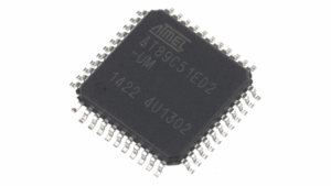
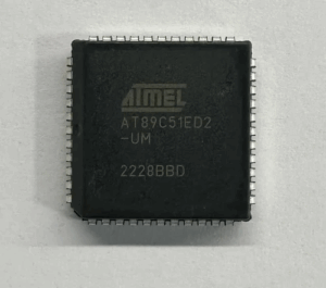
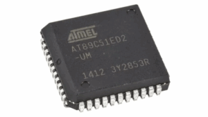
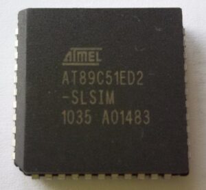
The effort to extract IC AT89C51ED2 code stands at the forefront of modern hardware reverse engineering and binary recovery technology. The AT89C51ED2 is a high-performance 8-bit microcontroller built on the 8051 architecture, developed by Atmel. It features 64KB of Flash memory, 2048 bytes of EEPROM, and an on-chip bootloader, making it a preferred choice for embedded industrial applications.
However, when a device integrator or engineer requires access to the embedded firmware, source code, or heximal program stored within the MCU, they often find themselves locked out. The AT89C51ED2 includes multiple layers of security: code protection bits, encrypted bootloader routines, and locked flash memory regions. These mechanisms make traditional access methods ineffective — and demand a more sophisticated strategy to crack, break, or recover the target data.
To extract the binary contents from a secured AT89C51ED2 chip, expert engineers employ invasive and non-invasive attack methods. One of the most advanced approaches is decapsulation, where the chip is physically stripped down using acid or plasma to expose the silicon die. Once opened, techniques such as laser probing, fault injection, or SEM imaging may be used to bypass or directly read the memory content.
Alternatively, power analysis or clock glitching can be used to decode the behavior of the microprocessor, attempting to find a vulnerability during startup or firmware validation. In rare cases, misconfigured bootloaders or debugging interfaces allow for partial access — enabling skilled operators to dump and restore fragments of the firmware archive.
One key challenge when attempting to extract IC AT89C51ED2 code is its protected architecture. This MCU is designed to erase the internal flash instantly if tampering is detected — a significant risk during any hack or decrypt operation. Timing, precision, and deep technical expertise are essential to avoid irreversible data loss.
Despite these barriers, successful recovery, replication, or duplication of the embedded file allows engineers to preserve critical legacy systems, troubleshoot black-box devices, or develop compatible clones.
In conclusion, the AT89C51ED2 represents a complex, highly secured MCU — but with the right techniques, tools, and patience, it is possible to extract IC AT89C51ED2 code and access its firmware — unlocking valuable insight hidden within its memory.
Extract IC AT89C51ED2 Code by disable the security fuse bit embedded inside the Microcontroller AT89C51ED2 and dump the heximal out from its flash and eeprom memory; The AT89C51RD2/ED2 core needs only 6 clock periods per machine cycle. This feature called ‘X2’ provides the following advantages:
Divide frequency crystals by 2 (cheaper crystals) while keeping same CPU power. Save power consumption while keeping same CPU power (oscillator power saving). Save power consumption by dividing dynamically the operating frequency by 2 in operating and idle modes when Extract mcu at89c52 hex.
Increase CPU power by 2 while keeping same crystal frequency. In order to keep the original C51 compatibility, a divider by 2 is inserted between the XTAL1 signal and the main clock input of the core (phase generator). This divider may be disabled by software if Extract microcontroller at89c55 code.
The clock for the whole circuit and peripherals is first divided by two before being used by the CPU core and the peripherals. This allows any cyclic ratio to be accepted on XTAL1 input. In X2 mode, as this divider is bypassed, the signals on XTAL1 must have a cyclic ratio between 40 to 60%.
Figure 5 shows the clock generation block diagram. X2 bit is validated on the rising edge of the XTAL1 ÷ 2 to avoid glitches when switching from X2 to STD mode. Figure 6 shows the switching mode waveforms. The X2 bit in the CKCON0 register allows a switch from 12 clock periods per instruction to 6 clock periods and vice versa.
The T0X2, T1X2, T2X2, UartX2, PcaX2, and WdX2 bits in the CKCON0 register (Table 16) and SPIX2 bit in the CKCON1 register (see Table 17) allows a switch from standard peripheral speed (12 clock periods per peripheral clock cycle) to fast peripheral speed (6 clock periods per peripheral clock cycle). These bits are active only in X2 mode.
As detailed in Section “Hardware Watchdog Timer”, page 86, the WDT generates a 96- clock period pulse on the RST pin. In order to properly propagate this pulse to the rest of the application in case of external capacitor or power-supply supervisor circuit, a 1 kΩ resistor must be added.
The POR/PFD function monitors the internal power-supply of the CPU core memories and the peripherals, and if needed, suspends their activity when the internal power supply falls below a safety threshold. This is achieved by applying an internal reset to them.
By gen erating the Re se t the Power Monito r insures a correct start up whe n AT89C51RD2/ED2 is powered up.
In order to startup and maintain the microcontroller in correct operating mode, VCC has to be stabilized in the VCC operating range and the oscillator has to be stabilized with a nominal amplitude compatible with logic level VIH/VIL. These parameters are controlled during the three phases: power-up, normal operation and power going down..
When the power is applied, the Power Monitor immediately asserts a reset. Once the internal supply after the voltage regulator reach a safety level, the power monitor then looks at the XTAL clock input. The internal reset will remain asserted until the Xtal1 levels are above and below VIH and VIL. Further more. An internal counter will count 1024 clock periods before the reset is de-asserted.
If the internal power supply falls below a safety level, a reset is immediately asserted.