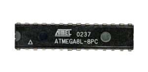
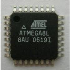
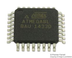
The effort to extract chip ATMEGA8L firmware is a highly technical process that involves breaching the embedded security of a locked, protected, or even encrypted microcontroller. The ATMEGA8L, a low-power CMOS 8-bit MCU from Microchip (formerly Atmel), is based on the AVR RISC architecture. It features 8KB of in-system programmable flash, 512B of EEPROM, and 1KB of SRAM, making it widely used in fields like consumer electronics, automotive systems, industrial automation, and IoT devices.

This microcontroller’s low-voltage operation (down to 2.7V) and versatile flash memory access make it attractive for cost-sensitive, power-efficient applications. But when a client needs to recover, copy, or restore the internal program, particularly when the original source is lost or the device is obsolete, the only option is to dump the firmware directly from the chip.
However, the ATMEGA8L is no ordinary target. It features fuse bits and lock bits that, when configured, make the device highly secured against external access. In this state, all traditional programmer tools are rendered useless for extracting the internal binary or heximal file.
To crack this chip, experts use advanced reverse engineering techniques:
-
Decapsulation: The chip package is chemically stripped to expose the silicon die, enabling optical or electronic probing of its internal memory structure.
-
Fault injection: High-precision glitches in voltage or clock signals are introduced to force the MCU into an insecure state.
-
Side-channel analysis: By observing electromagnetic emissions or power consumption during execution, attackers attempt to decode the firmware operations.
-
Protocol abuse: Rare bootloader modes or debug interfaces, if misconfigured, may be leveraged to hack into otherwise locked devices.
Each of these methods poses different challenges: die-layer complexity, fuse redundancy, or precise timing controls. The ATMEGA8L’s robust architecture resists naïve attempts to copy or clone the internal data, demanding in-depth microelectronic knowledge and specialized lab equipment.
Once successful, the extracted archive or dump can be analyzed to replicate behavior, migrate to another system, or perform critical firmware recovery in legacy deployments.
In essence, the mission to extract chip ATMEGA8L firmware is a sophisticated digital attack requiring a blend of physical science and firmware expertise. Its complexity lies not just in breaking the protection, but in preserving data integrity and functional restoration of valuable embedded logic.
Extract Chip ATMEGA8L Firmware from its flash memory and eeprom memory after crack MCU ATmega8L secured system, the security fuse bits can be disable by laser cutting;
The AVR core combines a rich instruction set with 32 general purpose working registers. All the 32 registers are directly connected to the Arithmetic Logic Unit (ALU), allowing two independent registers to be accessed in one single instruction executed in one clock cycle. The resulting architecture is more code efficient while achieving throughputs up to ten times faster than conventional CISC microcontrollers when extract mcu at89c52 hex.
The ATmega8 provides the following features: 8K bytes of In-System Programmable Flash with Read-While-Write capabilities, 512 bytes of EEPROM, 1K byte of SRAM, 23 general purpose I/O lines, 32 general purpose working registers, three flexible Timer/Counters with compare modes, internal and external interrupts, a serial programmable USART, a byte oriented Two-wire Serial Interface, a 6-channel ADC (eight channels in TQFP and QFN/MLF packages) with 10-bit accuracy, a programmable Watchdog Timer with Internal Oscillator, an SPI serial port, and five software selectable power saving modes. The Idle mode stops the CPU while allowing the SRAM, Timer/Counters, SPI port, and interrupt system to continue functioning when Extract microcontroller at89c55 code.
The Power-down mode saves the register contents but freezes the Oscillator, disabling all other chip functions until the next Interrupt or Hardware Reset. In Power-save mode, the asynchronous timer continues to run, allowing the user to maintain a timer base while the rest of the device is sleeping.
The ADC Noise Reduction mode stops the CPU and all I/O modules except asynchronous timer and ADC, to minimize switching noise during ADC conversions. In Standby mode, the crystal/resonator Oscillator is running while the rest of the device is sleeping. This allows very fast start-up combined with low-power consumption.
The device is manufactured using Atmel’s high density non-volatile memory technology. The Flash Program memory can be reprogrammed In-System through an SPI serial interface, by a conventional non-volatile memory programmer, or by an On-chip boot program running on the AVR core.
The boot program can use any interface to download the application program in the Application Flash memory. Software in the Boot Flash Section will continue to run while the Application Flash Section is updated, providing true Read-While-Write operation.
By combining an 8-bit RISC CPU with In-System Self-Programmable Flash on a monolithic chip, the Atmel ATmega8 is a powerful microcontroller that provides a highly-flexible and cost-effective solution to many embedded control applications.
The ATmega8 AVR is supported with a full suite of program and system development tools, including C compilers, macro assemblers, program debugger/simulators, In-Circuit Emulators, and evaluation kits.