Extract Chip ATmega164PA Code focuses on advanced reverse engineering techniques used to read out binary or heximal data from a secured ATmega164PA microcontroller. In many embedded products, the original firmware, source code, or program archive may be lost due to supplier changes, discontinued development teams, or legacy system aging. When the MCU is protected, encrypted, or locked, standard programmers cannot open or access its internal flash or EEPROM memory. Through controlled and professional reverse engineering, it becomes possible to extract critical firmware files, recover program data, and restore functional logic from the chip, enabling continued use or analysis of the embedded system.
Since the external memory is mapped after the internal memory as shown in Figure 14, the external memory is not addressed when addressing the first 8,704 bytes of data space.
It may appear that the first 8,704 bytes of the external memory are inaccessible (external memory addresses 0x0000 to 0x21FF). However, when connecting an external memory smaller than 64 KB, for example 32 KB, these locations are easily accessed simply by addressing from address 0x8000 to 0xA1FF.
Since the External Memory Address bit A15 is not connected to the external memory, addresses 0x8000 to 0xA1FF will appear as addresses 0x0000 to 0x21FF for the external memory.
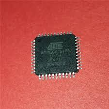
The ATmega164PA is a low-power variant of the classic AVR ATmega family, designed for improved energy efficiency while maintaining strong performance. It features ample flash memory, EEPROM, and SRAM, along with peripherals such as SPI, I²C, UART interfaces, multiple timers, PWM channels, and flexible GPIO configurations. These characteristics make the ATmega164PA microcontroller widely deployed in industrial automation equipment, smart meters, control panels, medical instruments, security systems, and long-life consumer electronics. In such applications, the firmware stored inside the MCU defines communication protocols, control algorithms, and safety logic, making the embedded program memory a core intellectual asset.
Addressing above address 0xA1FF is not recommended, since this will address an external memory location that is already accessed by another (lower) address. To the Application software, the external 32 KB memory will appear as one linear 32 KB address space from 0x2200 to 0xA1FF. This is illustrated in Figure 20.
Since the External Memory is mapped after the Internal Memory as shown in Figure 14,only 56KB of External Memory is available by default (address space 0x0000 to 0x21FF is reserved for internal memory). However, it is possible to take advantage of the entire External Memory by masking the higher address bits to zero.
This can be done by using the XMMn bits and control by software the most significant bits of the address. By setting Port C to output 0x00, and releasing the most significant bits for normal Port Pin operation, the Memory Interface will address 0x0000 – 0x2FFF. See the following code examples.
Care must be exercised using this option as most of the memory is masked away. Figure 21 presents the principal clock systems in the AVR and their distribution. All of the clocks need not be active at a given time. In order to reduce power consumption, the clocks to modules not being used can be halted by using different sleep modes, as described in “Power Management and Sleep Modes” on page 51. The clock systems are detailed below.
The CPU clock is routed to parts of the system concerned with operation of the AVR core. Examples of such modules are the General Purpose Register File, the Status Register and the data memory holding the Stack Pointer. Halting the CPU clock inhibits the core from performing general operations and calculations.
The I/O clock is used by the majority of the I/O modules, like Timer/Counters, SPI, and USART. The I/O clock is also used by the External Interrupt module, but note that some external interrupts are detected by asynchronous logic, allowing such interrupts to be detected even if the I/O clock is halted.
Also note that start condition detection in the USI module is carried out asynchronously when clkI/O is halted, TWI address recognition in all sleep modes.
The Flash clock controls operation of the Flash interface. The Flash clock is usually active simultaneously with the CPU clock. The Asynchronous Timer clock allows the Asynchronous Timer/Counter to be clocked directly from an external clock or an external 32 kHz clock crystal.
The dedicated clock domain allows using this Timer/Counter as a real-time counter even when the device is in sleep mode. The ADC is provided with a dedicated clock domain. This allows halting the CPU and I/O clocks in order to reduce noise generated by digital circuitry.
This gives more accurate ADC conversion results. The device has the following clock source options, selectable by Flash Fuse bits as shown below. The clock from the selected source is input to the AVR clock generator, and routed to the appropriate modules.
Attempting to hack, extract, or recover data from a secured ATmega164PA chip presents significant technical challenges. Protection fuse bits are intentionally designed to block readout of flash, EEPROM, and internal memory regions, preventing direct access to binary dumps or heximal files. Additional difficulties include encrypted data areas, sensitivity to voltage and clock conditions, and the risk of triggering irreversible memory erase mechanisms. Reverse engineering a protected or locked microcontroller therefore requires deep expertise in AVR architecture, memory mapping, and protection strategies. The objective is to open access to the required firmware data without damaging the chip or corrupting valuable program information.
The value of extracting ATmega164PA code lies in the tangible benefits it delivers to clients. By restoring firmware, program archives, or memory dumps from a locked MCU, companies can maintain legacy products, perform functional upgrades, or migrate designs to new hardware platforms. Recovering source-level logic from binary or flash data also supports troubleshooting, compliance verification, and controlled product duplication. Instead of redesigning an entire system from scratch, clients gain access to critical embedded data that preserves their original investment. Ultimately, professional reverse engineering of the ATmega164PA microprocessor transforms secured and inaccessible firmware into usable digital assets, delivering long-term technical and commercial advantages.