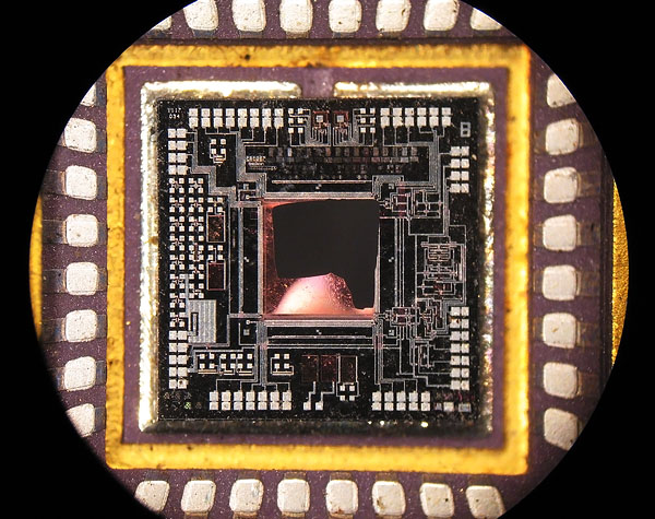
The ARM Microcontroller STM32F071R8 Flash Firmware can be duplicated after disable its readout protection fuse bit through MCU stm32f071r8 reverse technique; make stm32f071r8 microprocessor’s cloned unit by rewrite the heximal to new mcu;
The current consumption of the on-chip peripherals is given in Table 35. The MCU is placed under the following conditions:
- All I/O pins are in analog mode
- All peripherals are disabled unless otherwise mentioned
- The given value is calculated by measuring the current consumption
- with all peripherals clocked off
- with only one peripheral clocked on
- Ambient operating temperature and supply voltage conditions summarized in Table 21: Voltage characteristics
The power consumption of the digital part of the on-chip peripherals is given. The power consumption of the analog part of the peripherals (where applicable) is indicated in each related section of the datasheet.
In bypass mode the LSE oscillator is switched off and the input pin is a standard GPIO. The external clock signal has to respect the I/O characteristics in Section 6.3.14. However, the recommended clock input waveform is shown in Figure 15.