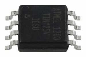
Read Chip ATtiny25V Software from encrypted flash memory, unlock mcu attiny25v flash memory and break off the security fuse bit of microcontroller attiny25v by focus ion beam;
Port B is a 6-bit bi-directional I/O port with internal pull-up resistors (selected for each bit). The Port B output buffers have symmetrical drive characteristics with both high sink and source capability. As inputs, Port B pins that are externally pulled low will source current if the pull-up resistors are activated.
The Port B pins are tri-stated when a reset condition becomes active, even if the clock is not running. Reset input. A low level on this pin for longer than the minimum pulse length will generate a reset, even if the clock is not running. The minimum pulse length is given in Table 23-3 on page 170. Shorter pulses are not guaranteed to generate a reset.
-
- Some of the Status Flags are cleared by writing a logical one to them. Note that, unlike most other AVRs, the CBI and SBI
- I/O Registers within the address range 0x00 – 0x1F are directly bit-accessible using the SBI and CBI instructions. In these
- For compatibility with future devices, reserved bits should be written to zero if accessed. Reserved I/O memory addresses should never be written. registers, the value of single bits can be checked by using the SBIS and SBIC instructions. instructions will only operation the specified bit, and can therefore be used on registers containing such Status Flags. The CBI and SBI instructions work with registers 0x00 to 0x1F only.
- I/O Registers within the address range 0x00 – 0x1F are directly bit-accessible using the SBI and CBI instructions. In these
- PLL not locking
When at frequencies below 6.0 MHz, the PLL will not lock
Problem fix / Workaround
When using the PLL, run at 6.0 MHz or higher
- EEPROM read from application code does not work in Lock Bit Mode 3
When the Memory Lock Bits LB2 and LB1 are programmed to mode 3, EEPROM read does not work from the application code.
Problem Fix/Work around
Do not set Lock Bit Protection Mode 3 when the application code needs to read from EEPROM.
- Reading EEPROM at low frequency may not work for frequencies below 900 kHz
Reading data from the EEPROM at low internal clock frequency may result in wrong data read.
Problem Fix/Workaround
Avoid using the EEPROM at clock frequency below 900kHz.
- Some of the Status Flags are cleared by writing a logical one to them. Note that, unlike most other AVRs, the CBI and SBI
-
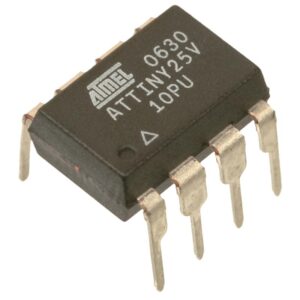
decode attiny25v microcontroller flash program and clone the firmware heximal to new attiny25v - Timer Counter 1 PWM output generation on OC1B – XOC1B does not work correctly
Timer Counter1 PWM output OC1B-XOC1B does not work correctly. Only in the case when the control bits, COM1B1 and COM1B0 are in the same mode as COM1A1 and COM1A0, respectively, the OC1B-XOC1B output works correctly
Problem Fix/Work around
The only workaround is to use same control setting on COM1A(1:0) and COM1B(1:0) control bits, see table 14-4 in the data sheet. The problem has been fixed for Tiny45 rev D.