Extract Microcontroller ATmega2560 flash memory firmware describes the controlled process of obtaining a complete binary or heximal representation of the internal program stored in a secured ATmega2560 microcontroller. As one of the most capable AVR-based MCUs, the ATmega2560 integrates a powerful 8-bit microprocessor core with up to 256 KB of on-chip flash, multiple banks of EEPROM, and extensive memory addressing capability. These features make it a cornerstone chip for complex embedded platforms.
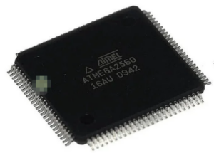
The ATmega2560 is widely recognized for its rich peripheral set, including multiple UARTs, SPI, I²C, advanced timers, and a large number of GPIOs. Because of this versatility, the MCU is deployed across many industries: industrial automation controllers, CNC and motion systems, laboratory instruments, data loggers, smart energy equipment, and embedded control boards used in education and prototyping. In most production environments, the device is configured as secured, protected, or fully locked to prevent unauthorized access to critical firmware and proprietary data.
XTAL1 and XTAL2 are the input and output, respectively, of an inverting amplifier which can be configured for use as an on-chip oscillator, as shown in Figure 1. Either a quartz crystal or ceramic resonator may be used.
When original source code or design files are missing, organizations may need to extract a reliable dump of the flash memory to understand system behavior. This is not a simple “open” operation. Security fuses, read-protection bits, and in some cases encrypted storage mechanisms are specifically designed to resist direct access. Attempting to bypass these controls without expertise can result in erased memory or a nonfunctional MCU, which is why professional reverse engineering practices are essential.
From a technical standpoint, the difficulty lies in accessing the flash and EEPROM contents without triggering protection responses. The process may involve carefully orchestrated recovery steps to restore a consistent file or structured archive from the device. While the terms hack or attack are sometimes used informally, legitimate services focus on compliant recovery scenarios such as maintenance, failure analysis, product migration, or long-term support for discontinued systems.
2. There are no requirements on the duty cycle of the external clock signal, since the input to the internal clocking circuitry is through a divide-by-two flip-flop, but minimum and maximum voltage high and low time specifications must be observed.
In idle mode, the CPU puts itself to sleep while all the on-chip peripherals remain active. The mode is invoked by software. The content of the on-chip RAM and all the special functions registers remain unchanged during this mode.
The idle mode can be terminated by any enabled interrupt or by a hardware reset. It should be noted that when idle is terminated by a hard ware reset, the device normally resumes program execution, from where it left off, up to two machine cycles before the internal reset algorithm takes control.
On-chip hardware inhibits access to internal RAM in this event, but access to the port pins is not inhibited. To eliminate the possibility of nated. The only exit from power down is a hardware reset. Reset redefines the SFRs but does not change the on-chip RAM.
The reset should not be activated before VCC is restored to its normal operating level and must be held active long enough to allow the oscillator to restart and stabilize.
On the chip are three lock bits which can be left unprogrammed (U) or can be programmed (P) to obtain the additional features listed in the table below:
When lock bit 1 is programmed, the logic level at the EA pin is sampled and latched during reset. If the device is powered up without a reset, the latch initializes to a random value, and holds that value until reset is activated. It is necessary that the latched value of EA be in agreement with the current logic level at that pin in order for the device to function properly.
The business value of extracting ATmega2560 firmware is significant. Clients gain the ability to preserve legacy products, reproduce existing functionality, or migrate an embedded design to new hardware without rewriting the entire application. Access to the recovered program and memory data also supports debugging, regulatory compliance, and lifecycle management. In many cases, the recovered archive becomes a strategic asset that prevents vendor lock-in and reduces redevelopment costs.
In summary, extracting flash memory firmware from a locked ATmega2560 MCU is a specialized engineering task. When performed responsibly, it delivers continuity, protects intellectual investment, and enables organizations to extend the operational life of critical embedded systems with confidence.