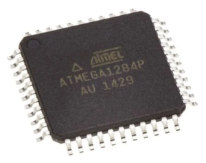
In embedded product maintenance and failure analysis, the need to read microcontroller ATmega1284P flash memory often arises when critical firmware files are no longer available from the original developer. The ATmega1284P MCU stores its operational program inside internal flash memory, supported by EEPROM and SRAM for parameter and runtime data handling. When the chip is configured as secured, protected, encrypted, or locked, standard programming interfaces cannot open or access its internal memory space. This restriction prevents direct retrieval of the binary or heximal file that defines the system’s behavior. Under such circumstances, controlled reverse engineering becomes the only viable path to extract and recover the firmware archive from the microprocessor.
ATmega1284P 마이크로컨트롤러 플래시 메모리 복구 프로젝트는 원본 소스 코드나 프로그램 파일을 분실한 후, 보안 및 암호화된 칩에서 펌웨어를 해킹, 추출 또는 복구해야 하는 경우에 자주 발생합니다. 보호되거나 잠긴 MCU는 외부 읽기 명령을 비활성화하거나, 내부 메모리 세그먼트를 암호화하거나, 무단 액세스가 감지되면 자동 삭제 메커니즘을 작동시킬 수 있습니다. ATmega1284P를 역설계하려면 제한된 플래시 메모리 영역을 조심스럽게 열고 EEPROM 데이터를 손상시키거나 마이크로컨트롤러를 손상시키지 않고 완전한 바이너리 또는 16진수 덤프를 추출하기 위한 전문적인 기술이 필요합니다. 기술적 과제로는 읽기 방지 퓨즈 구성 탐색, 클록 및 전압 파라미터 안정화, 암호화된 펌웨어 블록 보존, 원시 데이터로부터 일관성 있는 메모리 파일 재구성 등이 있습니다. 목표는 칩 내부에 저장된 원래 프로그램 구조를 반영하는 정확한 펌웨어 아카이브를 복원하는 것입니다. 보호된 ATmega1284P MCU에서 펌웨어를 복구하고 복원하는 능력은 운영 및 상업적으로 상당한 이점을 제공합니다. 검증된 바이너리 파일이나 플래시 메모리 덤프를 추출함으로써 고객은 중단된 생산 라인을 재개하고, 기존 하드웨어 플랫폼을 유지하며, 복잡한 소스 코드를 다시 작성하지 않고도 임베디드 설계를 최신 마이크로컨트롤러로 마이그레이션할 수 있습니다. 복구된 데이터 아카이브에 대한 접근은 디버깅, 규정 준수 검증, 성능 최적화 및 장기적인 제품 수명 주기 관리를 지원합니다. 기업은 전체 시스템을 재개발하는 대신 복구된 펌웨어를 활용하여 지적 재산을 보호하고 사업 연속성을 보장할 수 있습니다. 궁극적으로 ATmega1284P 플래시 읽기 서비스는 잠겨 접근할 수 없는 칩을 복구 가능한 디지털 자산으로 변환하여 기술적 복원력을 강화하고 보안 펌웨어 시스템에 내재된 가치를 보존합니다.
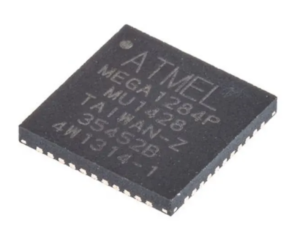
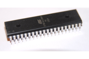
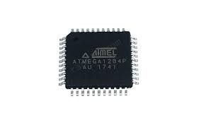
Technically, the ATmega1284P microcontroller is built on the AVR 8-bit RISC core and offers 128KB of flash program memory, generous SRAM capacity, and non-volatile EEPROM storage. It integrates dual USART channels, SPI, TWI (I²C), timers with PWM outputs, ADC modules, watchdog circuitry, and extensive GPIO resources. These features make the chip suitable for industrial automation controllers, communication gateways, smart metering equipment, environmental monitoring devices, robotics platforms, and sophisticated consumer electronics. In these systems, the MCU acts as the central processing unit, continuously executing firmware instructions and managing secure data exchange. The internal memory effectively serves as a structured data archive containing application logic, calibration constants, and system configuration.
Most port pins have alternate functions in addition to being general digital I/Os. Figure 37 shows how the port pin control signals from the simplified Figure 34 can be overridden by alternate functions. The overriding signals may not be present in all port pins, but the figure serves as a generic description applicable to all port pins in the AVR microcontroller family.
Việc đọc dữ liệu Flash từ vi điều khiển ATmega1284P thường phát sinh khi các tổ chức cần phải can thiệp, trích xuất hoặc khôi phục firmware từ một chip được bảo mật và mã hóa sau khi mất mã nguồn hoặc tệp chương trình gốc. Một MCU được bảo vệ hoặc khóa có thể vô hiệu hóa các lệnh đọc bên ngoài, mã hóa các phân đoạn bộ nhớ trong hoặc kích hoạt cơ chế xóa tự động khi phát hiện truy cập trái phép. Phân tích ngược ATmega1284P đòi hỏi chuyên môn cao để mở cẩn thận các vùng bộ nhớ flash bị hạn chế và trích xuất bản sao nhị phân hoặc thập lục phân hoàn chỉnh mà không làm hỏng dữ liệu EEPROM hoặc làm hỏng vi điều khiển. Các thách thức kỹ thuật bao gồm điều hướng cấu hình cầu chì bảo vệ đọc, ổn định các thông số xung nhịp và điện áp, bảo tồn các khối firmware được mã hóa và tái tạo một tệp bộ nhớ mạch lạc từ dữ liệu thô. Mục tiêu là khôi phục một kho lưu trữ firmware chính xác phản ánh cấu trúc chương trình gốc được lưu trữ bên trong chip. Khả năng khôi phục firmware từ MCU ATmega1284P được bảo vệ mang lại những lợi thế đáng kể về mặt hoạt động và thương mại. Bằng cách trích xuất tệp nhị phân đã được xác minh hoặc bản sao bộ nhớ flash, khách hàng có thể tiếp tục các dây chuyền sản xuất bị tạm dừng, duy trì các nền tảng phần cứng cũ và di chuyển các thiết kế nhúng sang các vi điều khiển được cập nhật mà không cần viết lại mã nguồn phức tạp. Việc truy cập vào kho dữ liệu đã được phục hồi hỗ trợ gỡ lỗi, xác thực tuân thủ, tối ưu hóa hiệu suất và quản lý vòng đời sản phẩm dài hạn. Thay vì đầu tư vào việc phát triển lại toàn bộ hệ thống, các doanh nghiệp có thể tận dụng phần mềm đã được khôi phục để bảo vệ tài sản trí tuệ và đảm bảo tính liên tục. Cuối cùng, dịch vụ Đọc Flash Vi điều khiển ATmega1284P biến một con chip bị khóa và không thể truy cập thành một tài sản kỹ thuật số có thể phục hồi, tăng cường khả năng phục hồi kỹ thuật và bảo toàn giá trị được nhúng bên trong các hệ thống phần mềm được bảo mật.
When this bit is written to one, the pull-ups in the I/O ports are disabled even if the DDxn and PORTxn Registers are configured to enable the pull-ups ({DDxn, PORTxn} = 0b01).
See “Configuring the Pin” on page 82 for more details about this feature. OC0A, Output Compare Match A output: The PB7 pin can serve as an external output for the Timer/Counter0 Output Compare. The pin has to be configured as an output (DDB7 set “one”) to serve this function. The OC0A pin is also the output pin for the PWM mode timer function.
OC1C, Output Compare Match C output: The PB7 pin can serve as an external output for the Timer/Counter1 Output Compare C. The pin has to be configured as an output (DDB7 set (one)) to serve this function. The OC1C pin is also the output pin for the PWM mode timer function.
PCINT7, Pin Change Interrupt source 7: The PB7 pin can serve as an external interrupt source.
OC1B/PCINT6, Bit 6
OC1B, Output Compare Match B output: The PB6 pin can serve as an external output for the Timer/Counter1 Output Compare B. The pin has to be configured as an output (DDB6 set (one)) to serve this function. The OC1B pin is also the output pin for the PWM mode timer function.
PCINT6, Pin Change Interrupt source 6: The PB7 pin can serve as an external interrupt source.
OC1A/PCINT5, Bit 5
OC1A, Output Compare Match A output: The PB5 pin can serve as an external output for the Timer/Counter1 Output Compare A. The pin has to be configured as an output (DDB5 set (one)) to serve this function. The OC1A pin is also the output pin for the PWM mode timer function.
PCINT5, Pin Change Interrupt source 5: The PB7 pin can serve as an external interrupt source.
OC2A/PCINT4, Bit 4
OC2A, Output Compare Match output: The PB4 pin can serve as an external output for the Timer/Counter2 Output Compare. The pin has to be configured as an output (DDB4 set (one)) to serve this function. The OC2A pin is also the output pin for the PWM mode timer function.
Read Microcontroller ATmega1284P Flash projects frequently arise when organizations must hack, extract, or recover firmware from a secured and encrypted chip after losing the original source code or program file. A protected or locked MCU may disable external read commands, encrypt internal memory segments, or trigger automatic erase mechanisms when unauthorized access is detected. Reverse engineering the ATmega1284P requires specialized expertise to carefully open restricted flash memory regions and extract a complete binary or heximal dump without corrupting EEPROM data or damaging the microcontroller. Technical challenges include navigating read-protection fuse configurations, stabilizing clock and voltage parameters, preserving encrypted firmware blocks, and reconstructing a coherent memory file from raw data. The objective is to restore an accurate firmware archive that reflects the original program structure stored inside the chip. The ability to recover and restore firmware from a protected ATmega1284P MCU provides significant operational and commercial advantages. By extracting a verified binary file or flash memory dump, clients can resume suspended production lines, maintain legacy hardware platforms, and migrate embedded designs to updated microcontrollers without rewriting complex source code. Access to recovered data archives supports debugging, compliance validation, performance optimization, and long-term product lifecycle management. Instead of investing in complete system redevelopment, businesses can leverage restored firmware to protect intellectual property and ensure continuity. Ultimately, Read Microcontroller ATmega1284P Flash services transform a locked and inaccessible chip into a recoverable digital asset, strengthening technical resilience and preserving the embedded value contained within secured firmware systems.
PCINT4, Pin Change Interrupt source 4: The PB7 pin can serve as an external interrupt source.
MISO/PCINT3 – Port B, Bit 3
MISO: Master Data input, Slave Data output pin for SPI channel. When the SPI is enabled as a master, this pin is configured as an input regardless of the setting of DDB3. When the SPI is enabled as a slave, the data direction of this pin is controlled by DDB3. When the pin is forced to be an input, the pull-up can still be controlled by the PORTB3 bit.
PCINT3, Pin Change Interrupt source 3: The PB7 pin can serve as an external interrupt source when Read Microcontroller.
MOSI/PCINT2 – Port B, Bit 2
MOSI: SPI Master Data output, Slave Data input for SPI channel. When the SPI is enabled as a slave, this pin is configured as an input regardless of the setting of DDB2. When the SPI is enabled as a master, the data direction of this pin is controlled by DDB2. When the pin is forced to be an input, the pull-up can still be controlled by the PORTB2 bit.
PCINT2, Pin Change Interrupt source 2: The PB7 pin can serve as an external interrupt source.
SCK/PCINT1 – Port B, Bit 1
SCK: Master Clock output, Slave Clock input pin for SPI channel. When the SPI is enabled as a slave, this pin is configured as an input regardless of the setting of DDB1. When the SPI0 is enabled as a master, the data direction of this pin is controlled by DDB1. When the pin is forced to be an input, the pull-up can still be controlled by the PORTB1 bit.
When organizations attempt to hack or open a locked ATmega1284P chip to recover lost source code or restore discontinued production, several technical barriers emerge. Protection fuse bits can block read access to flash and EEPROM memory, while certain secured configurations may automatically erase data if unauthorized access is detected. Reverse engineering a protected microcontroller therefore requires a highly controlled process to extract a consistent binary dump without corrupting the firmware. Engineers must carefully manage electrical stability, timing synchronization, and memory mapping to preserve encrypted or protected regions. The goal is not merely to copy data, but to reconstruct a usable program file or heximal archive that accurately reflects the original memory structure inside the MCU.
Successfully reading and restoring ATmega1284P flash memory delivers measurable value to clients. By recovering firmware and extracting a validated binary file, companies can resume production, repair legacy equipment, and migrate existing designs to new hardware platforms without rebuilding the entire system from scratch. Access to a complete memory dump enables firmware analysis, debugging, and compliance verification while safeguarding intellectual property. Instead of accepting costly redesign or product obsolescence, businesses can restore operational continuity through professional microcontroller recovery services. Ultimately, reading microcontroller ATmega1284P flash from a secured chip transforms a locked device into a recoverable technical resource, preserving embedded program assets and extending product lifecycle in competitive industries.
रीड माइक्रोकंट्रोलर ATmega1284P फ्लैश प्रोजेक्ट अक्सर तब आते हैं जब कंपनियों को ओरिजिनल सोर्स कोड या प्रोग्राम फ़ाइल खोने के बाद किसी सुरक्षित और एन्क्रिप्टेड चिप से फर्मवेयर को हैक करना, निकालना या रिकवर करना होता है। एक सुरक्षित या लॉक किया गया MCU बाहरी रीड कमांड को बंद कर सकता है, अंदरूनी मेमोरी सेगमेंट को एन्क्रिप्ट कर सकता है, या बिना इजाज़त एक्सेस का पता चलने पर ऑटोमैटिक इरेज़ मैकेनिज्म को चालू कर सकता है। ATmega1284P की रिवर्स इंजीनियरिंग के लिए खास जानकारी की ज़रूरत होती है ताकि रिस्ट्रिक्टेड फ्लैश मेमोरी रीजन को ध्यान से खोला जा सके और EEPROM डेटा को खराब किए बिना या माइक्रोकंट्रोलर को नुकसान पहुँचाए बिना एक पूरा बाइनरी या हेक्सिमल डंप निकाला जा सके। टेक्निकल चुनौतियों में रीड-प्रोटेक्शन फ्यूज कॉन्फ़िगरेशन को नेविगेट करना, क्लॉक और वोल्टेज पैरामीटर को स्थिर करना, एन्क्रिप्टेड फर्मवेयर ब्लॉक को बचाना और रॉ डेटा से एक सही मेमोरी फ़ाइल को फिर से बनाना शामिल है। इसका मकसद एक सटीक फर्मवेयर आर्काइव को रिस्टोर करना है जो चिप के अंदर स्टोर ओरिजिनल प्रोग्राम स्ट्रक्चर को दिखाता है। एक सुरक्षित ATmega1284P MCU से फर्मवेयर को रिकवर और रिस्टोर करने की क्षमता ऑपरेशनल और कमर्शियल दोनों तरह के बड़े फायदे देती है। वेरिफाइड बाइनरी फ़ाइल या फ्लैश मेमोरी डंप निकालकर, क्लाइंट रुकी हुई प्रोडक्शन लाइन फिर से शुरू कर सकते हैं, पुराने हार्डवेयर प्लेटफॉर्म बनाए रख सकते हैं, और मुश्किल सोर्स कोड को दोबारा लिखे बिना एम्बेडेड डिज़ाइन को अपडेटेड माइक्रोकंट्रोलर में माइग्रेट कर सकते हैं। रिकवर किए गए डेटा आर्काइव तक पहुंच डीबगिंग, कंप्लायंस वैलिडेशन, परफॉर्मेंस ऑप्टिमाइजेशन और लंबे समय तक चलने वाले प्रोडक्ट लाइफसाइकल मैनेजमेंट को सपोर्ट करती है। पूरे सिस्टम रीडेवलपमेंट में इन्वेस्ट करने के बजाय, बिज़नेस इंटेलेक्चुअल प्रॉपर्टी की सुरक्षा और कंटिन्यूटी सुनिश्चित करने के लिए रिस्टोर किए गए फर्मवेयर का इस्तेमाल कर सकते हैं। आखिर में, रीड माइक्रोकंट्रोलर ATmega1284P फ्लैश सर्विस एक लॉक और इनएक्सेसिबल चिप को रिकवर करने लायक डिजिटल एसेट में बदल देती है, जिससे टेक्निकल रेजिलिएंस मजबूत होता है और सुरक्षित फर्मवेयर सिस्टम में मौजूद एम्बेडेड वैल्यू बनी रहती है।