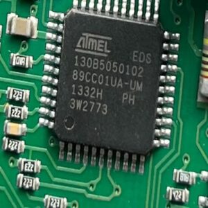
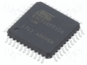
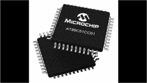
The process to read microcontroller AT89C51CC01 flash represents a critical challenge in the world of embedded security, particularly when the chip in question is secured, encrypted, or otherwise protected. The AT89C51CC01, manufactured by Atmel (now part of Microchip Technology), is a powerful 8-bit MCU based on the 8051 core. It integrates USB capabilities, EEPROM, and 32KB of on-chip flash memory, making it ideal for automotive and industrial control systems.
However, when a firmware or binary needs to be extracted from this chip — for example, for cloning, reverse engineering, or restoring legacy systems — engineers face serious barriers. This microcontroller features security lock bits and code protection, which, when enabled, prevent conventional access to the internal memory, flash, or EEPROM contents.
To dump the program data or source code from a secured AT89C51CC01, one must attempt sophisticated attack vectors. Common techniques include:
-
Decapsulation: Physically removing the chip’s packaging to expose the silicon die, which enables optical probing or laser fault injection.
-
Voltage glitching and clock fault injection: Introducing faults into the chip’s normal operation to bypass the security state.
-
Side-channel attacks: Monitoring power consumption or electromagnetic emissions to decode internal operations.
-
Bootloader abuse or debug interface exploitation (if not disabled): Leveraging known vulnerabilities to gain partial access.
These techniques require a deep understanding of semiconductor behavior and specialized equipment. The process to crack or break through these defenses is both expensive and time-consuming — especially with locked or encrypted firmware.
Despite the obstacles, successfully retrieving a heximal or binary archive from such a chip allows engineers to recover, replicate, or duplicate valuable legacy code. The dumped file can be analyzed to understand proprietary logic, reverse firmware behavior, or clone the original microprocessor setup.
What sets the AT89C51CC01 apart is not just its technical features, but the difficulties encountered during chip-level hacking. This chip’s robust security and integrated features make it resistant to casual copying or dumping efforts, demanding expert-level reverse engineering capabilities.
In conclusion, to read microcontroller AT89C51CC01 flash from a secured device is a high-skill endeavor that involves an arsenal of advanced methods to decrypt and recover the internal data — a task where knowledge, precision, and patience are essential.
Read Microcontroller AT89C51CC01 Flash content and copy MCU firmware into other blank AT89C51CC01, decapsulate the silicon package of MCU and get access to the internal databus of chip through crack MCU tamper resistance system.
The T89C51CC01 core needs only 6 clock periods per machine cycle. This feature, called ”X2”, provides the following advantages:
Divides frequency crystals by 2 (cheaper crystals) while keeping the same CPU power. Saves power consumption while keeping the same CPU power (oscillator power saving). Saves power consumption by dividing dynamic operating frequency by 2 in operating and idle modes. Increases CPU power by 2 while keeping the same crystal frequency.
In order to keep the original C51 compatibility, a divider-by-2 is inserted between the XTAL1 signal and the main clock input of the core (phase generator). This divider may be disabled by the software.
An extra feature is available to start after Reset in the X2 mode. This feature can be enabled by a bit X2B in the Hardware Security Byte. This bit is described in the section “In-System-Programming” if extract Microcontroller at89c55 code.
The X2 bit in the CKCON register (see Table 13) allows switching from 12 clock cycles per instruction to 6 clock cycles and vice versa. At reset, the standard speed is activated (STD mode).
Setting this bit activates the X2 feature (X2 mode) for the CPU Clock only (see Figure 5.).
The Timers 0, 1 and 2, Uart, PCA, Watchdog or CAN switch in X2 mode only if the corresponding bit is cleared in the CKCON register. The clock for the whole circuit and peripheral is first divided by two before being used by the CPU core and peripherals. This allows any cyclic ratio to be accepted on the XTAL1 input. In X2 mode, as this divider is bypassed, the signals on XTAL1 must have a cyclic ratio between 40 to 60%. Figure 5. shows the clock generation block diagram.
The X2 bit is validated on the XTAL1÷2 rising edge to avoid glitches when switching from the X2 to the STD mode. Figure 6 shows the mode switching waveforms.
Two power reduction modes are implemented in the T89C51CC01: the Idle mode and the Power-down mode. These modes are detailed in the following sections. In addition to these power reduction modes, the clocks of the core and peripherals can be dynamically divided by 2 using the X2 Mode detailed in Section “Clock”.
In order to start-up (cold reset) or to restart (warm reset) properly the microcontroller, a high level has to be applied on the RST pin. A bad level leads to a wrong initialisation of the internal registers like SFRs, PC, etc. and to unpredictable behavior of the microcontroller. A warm reset can be applied either directly on the RST pin or indirectly by an internal reset source such as a watchdog, PCA, timer, etc if extract chip embedded firmware.
Two conditions are required before enabling a CPU start-up: VDD must reach the specified VDD range, The level on xtal1 input must be outside the specification (VIH, VIL). If one of these two conditions are not met, the microcontroller does not start correctly and can execute an instruction fetch from anywhere in the program space. An active level applied on the RST pin must be maintained until both of the above conditions are met. A reset is active when the level VIH1 is reached and when the pulse width covers the period of time where VDD and the oscillator are not stabilized. Two parameters have to be taken into account to determine the reset pulse width:
VDD rise time (vddrst),
Oscillator startup time (oscrst).
To determine the capacitor the highest value of these two parameters has to be chosen.
The reset circuitry is shown in Figure 7 after Read Microcontroller.