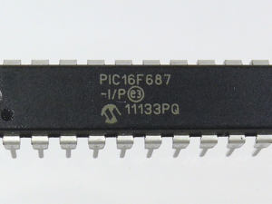
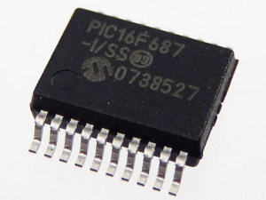
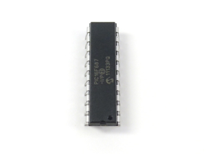
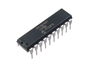
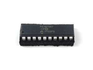
In the contemporary world of industrial automation and smart electronics, maintaining legacy infrastructure requires innovative engineering strategies. When a critical control unit fails and the original design schematics are entirely lost, the capability to Read Microchip PIC16F687 Flash memory becomes an indispensable asset for recovery teams. The PIC16F687 is a highly efficient 20-pin Flash-based MCU equipped with a precise internal oscillator, up to 18 I/O pins, and a robust synchronous serial port capable of managing complex communications. Due to its cost-effective footprint and reliable performance, this specific microcontroller is heavily integrated into commercial refrigeration control boards, smart security sensors, and automated industrial conveyor line modules. However, when these older setups require firmware patches or physical replication, engineers must find non-destructive ways to open, hack, or reverse engineering the system. Accessing the embedded intelligence of a discontinued chip is often the only viable strategy left to prevent complete operational stagnation.
Executing any instruction with the PCL register as the destination simultaneously causes the Program Counter PC<12:8> bits (PCH) to be replaced by the contents of the PCLATH register.
This allows the entire contents of the program counter to be changed by writing the desired upper 5 bits to the PCLATH register. When the lower 8 bits are written to the PCL register, all 13 bits of the program counter will change to the values contained in the PCLATH register and those being written to the PCL register. A computed GOTO is accomplished by adding an offset to the program counter (ADDWF PCL). Care should be exercised when jumping into a look-up table or program branch table (computed GOTO) by modifying the PCL register.
Assuming that PCLATH is set to the table start address, if the table length is greater than 255 instructions or if the lower 8 bits of the memory address rolls over from 0xFF to 0x00 in the middle of the table, then PCLATH must be incremented for each address rollover that occurs between the table beginning and the target location within the table. For more information refer to Application Note AN556, “Implementing a Table Read” (DS00556). The INDF register is not a physical register. Addressing PCLATH the INDF register will cause indirect addressing.
Indirect addressing is possible by using the IND register. Any instruction using the INDF register actually accesses data pointed to by the File Select Register (FSR). Reading INDF itself indirectly will produce 00h. Writing to the INDF register indirectly results in a no operation (although Status bits may be affected). An effective 9-bit address is obtained by concatenating the 8-bit FSR and the IRP bit of the STATUS register, as shown in Figure 2-10. A simple program to clear RAM location 20h-2Fh using indirect addressing is shown in Example 2-1.
The technical journey of bypassing hardware restrictions on a secured, protected, or locked semiconductor requires an intimate understanding of modern silicon layouts. When specialized engineers attempt to extract, recover, or restore functional instructions from a hardened target, they aim directly for the raw binary or heximal file stored within the inner silicon matrix. This highly focused operation is explicitly designed to dump the flash program memory blocks and the internal eeprom storage, which together serve as the underlying data archive for the entire machine. By successfully lifting this embedded code, engineering firms can analyze machine behaviors and study system dependencies without access to the original source code. Because the native microprocessor leverages strict hardware-level fuses to actively block unauthorized read commands, executing a pristine dump requires specialized signal exploitation methods that trick the MCU into exposing its payload without triggering a self-erase security trip.
Overcoming these internal silicone guardrails presents massive technical challenges and demands extreme procedural caution. Factory-level protection schemes on a premier microprocessor utilize hidden security meshes, internal clock monitors, and voltage spike filters that are specifically programmed to permanently erase the internal flash and eeprom matrices if any external tampering is detected. If an unauthorized tool applies incorrect electrical tolerances during a read sequence, the chip will immediately enter a permanent lockdown mode, destroying the exact data asset you are trying to isolate. Why do commercial entities choose to navigate these complex risks to open a protected architecture? The necessity arises because original component manufacturers frequently declare bankruptcy, stop supporting older product lines, or withhold proprietary software files, leaving critical industrial infrastructure entirely stranded when a single secured component experiences a physical hardware fault.
Ultimately, obtaining a flawless heximal or binary file from an encrypted integrated circuit yields profound commercial benefits for our clients. By utilizing highly controlled hardware reverse engineering workflows, enterprise asset managers can effectively immunize their operations against vendor lock-in and forced machinery upgrades. Having an uninhibited look into the device firmware archive gives engineering teams the freedom to patch latent software vulnerabilities, clone end-of-life parts onto modern, sustainable circuit boards, and maintain rigorous long-term regulatory compliance. This specialized technical approach effectively converts an inaccessible, locked hardware obstacle back into a fully visible, documented software asset—drastically minimizing unexpected downtime, bypassing unpredictable global supply chain constraints, and guaranteeing business continuity for years to come.