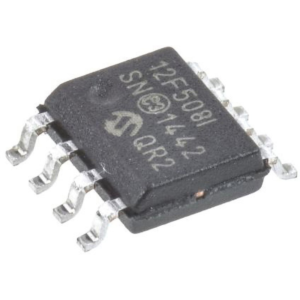
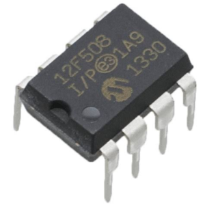
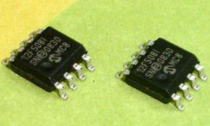
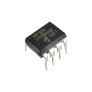
The PIC12F508 microcontroller is a compact 8-bit MCU designed for cost-sensitive and space-constrained embedded applications. With its minimal pin count, internal oscillator, and efficient instruction set, this chip is widely used in consumer electronics, power control modules, lighting systems, small automation devices, and portable equipment. Despite its simplicity, the PIC12F508 often executes critical firmware that governs device behavior at a fundamental level. In many production environments, manufacturers configure the chip in a secured or locked state to protect intellectual property, ensuring that the program, source code, and internal data stored in memory cannot be easily accessed. As a result, attempting to open or read the binary or heximal file from such a protected MCU presents a significant technical barrier.
In practical engineering cases, the requirement to hack, extract, recover, restore, or reverse engineering a PIC12F508 arises when essential firmware or design documentation is unavailable. Over time, original source code, archive files, or program backups may be lost, yet the embedded system continues to rely on the MCU for operation. Accessing the internal memory of a protected chip involves retrieving binary data, EEPROM content, or program instructions while navigating built-in protection mechanisms. Engineers must perform a controlled dump of the firmware and memory file, ensuring that the extracted data remains consistent and usable. The goal is to rebuild a complete archive of the microcontroller’s program logic without compromising the integrity of the chip or its stored data.
The code for these functions is available on our website www.microchip.com. The code will be accessed by either including the source code FL51XINC.ASM or by linking FLASH5IX.ASM. It is very important to check the return codes when using these calls, and retry the operation if unsuccessful. Unsuccessful return codes occur when the EE data memory is busy with the previous write, which can take up to 4 mS. SDA is a bi-directional pin used to transfer addresses and data into and data out of the device. For normal data transfer SDA is allowed to change only during SCL low. Changes during SCL high are reserved for indicating the START and STOP conditions. The EEPROM interface is a 2-wire bus protocol consisting of data (SDA) and a clock (SCL). Although these lines are mapped into the GPIO register, they are not accessible as external pins; only to the internal EEPROM peripheral.
SDA and SCL operation is also slightly different than GPO-GP5 as listed below. Namely, to avoid code overhead in modifying the TRIS register, both SDA and SCL are always output.
To read data from the EEPROM peripheral requires outputting a ‘1’ on SDA placing it in high-Z state, where only the internal 100K pull-up is active on the SDA line. This code must reside in the lower half of a page. The code achieves it’s small size without additional calls through the use of a sequencing table. The table is a list of procedures that must be called in order. The table uses an ADDWF PCL,F instruction, effectively a computed goto, to sequence to the next procedure. However the ADDWF PCL,F instruction yields an 8 bit address,
The following bus protocol is to be used with the EEPROM data memory.
- Data transfer may be initiated only when the bus is not busy.
During data transfer, the data line must remain stable whenever the clock line is HIGH. Changes in the data line while the clock line is HIGH will be interpreted as a period of the clock signal. There is one bit of data per clock pulse. Each data transfer is initiated with a START condition and terminated with a STOP condition. The number of the data bytes transferred between the START and STOP conditions is determined by the master device and is theoretically unlimited.
From a technical execution standpoint, reading MCU PIC12F508 program data from a secured, protected, encrypted, or locked device requires overcoming several layers of hardware-level restrictions. To hack, extract, recover, open, restore, or reverse engineering the MCU, specialists must address read-protection bits that block access to firmware, source code, binary, heximal program file, and internal memory data structures. The chip may contain critical information distributed across flash or EEPROM, and obtaining a reliable dump of this archive demands precise handling. Challenges such as signal instability, partial data retrieval, and risk of corruption must be carefully managed. Ensuring the accuracy of recovered firmware, program memory, and data archive is essential for reconstructing the original functionality of the microcontroller.
Successfully extracting and restoring data from a locked PIC12F508 chip delivers meaningful benefits to clients across multiple industries. By recovering firmware, binary files, and source code archives, businesses can replicate or duplicate the MCU’s behavior, enabling continued maintenance and support of legacy systems. Reverse engineering provides visibility into the internal program structure, allowing engineers to optimize, troubleshoot, or migrate the design to more advanced microcontrollers or microprocessors. This capability is particularly valuable in long-lifecycle products where replacement is costly or impractical. Ultimately, the ability to restore and reuse data from a secured MCU reduces operational risk, lowers maintenance costs, and extends the service life of critical equipment, transforming inaccessible embedded systems into sustainable and manageable assets.