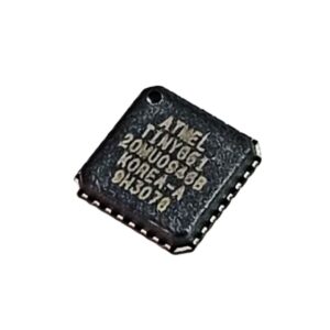
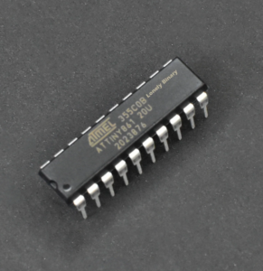
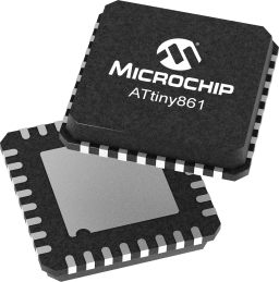
The ability to read IC ATtiny861 software is increasingly important for companies maintaining or upgrading embedded systems built on legacy AVR platforms. The ATtiny861 is a compact yet capable 8-bit microcontroller (MCU) that integrates flash program memory, internal EEPROM, SRAM, high-resolution timers, PWM channels, and flexible I/O resources. These features make the chip well suited for cost-sensitive and space-constrained designs in industrial control, motor drivers, power tools, consumer electronics, lighting systems, and intelligent sensor modules.
In many real-world projects, the complete firmware or source code exists only inside the microcontroller chip itself. When documentation has been lost, suppliers have changed, or products have been discontinued, it becomes necessary to extract, recover, or open the embedded binary or heximal program directly from the ATtiny861. This process enables access to valuable operational data, configuration tables, and logic sequences stored in flash, EEPROM, and other internal memory areas.
Read IC ATtiny861 Software from its flash memory after unlock atmel microcontroller attiny861 fuse bit and then recover the embedded heximal from mcu attiny861 flash memory;
Reset input. A high on this pin for two machine cycles while the oscillator is running resets the device. This pin drives High for 98 oscillator periods after the Watchdog times out. The DISRTO bit in SFR AUXR (address 8EH) can be used to disable this feature. In the default state of bit DISRTO, the RESET HIGH out feature is enabled.
Address Latch Enable is an output pulse for latching the low byte of the address during accesses to external memory. This pin is also the program pulse input (PROG) during Flash programming.
In normal operation, ALE is emitted at a constant rate of 1/6 the oscillator frequency and may be used for external timing or clocking purposes. Note, however, that one ALE pulse is skipped during each access to external data memory.
Reading software from a secured, protected, encrypted, or locked ATtiny861 is technically challenging. The device implements readout protection mechanisms designed to prevent unauthorized access to its internal file structure. Standard programming interfaces are blocked once protection fuses are enabled, making a simple dump of the firmware impossible. Successfully restoring a usable archive requires deep knowledge of AVR microprocessor architecture and disciplined reverse engineering techniques, rather than generic tools.
Although the term hack is often used casually, professional extraction is a controlled engineering activity. The objective is not to bypass security irresponsibly, but to restore legitimate software assets for maintenance, analysis, or redevelopment. During this process, engineers focus on preserving firmware integrity, reconstructing accurate source code–level logic where possible, and ensuring that the recovered program can be validated and reused safely.
If desired, ALE operation can be disabled by setting bit 0 of SFR location 8EH. With the bit set, ALE is active only during a MOVX or MOVC instruction. Otherwise, the pin is weakly pulled high. Setting the ALE-disable bit has no effect if the microcontroller is in external execution mode. Program Store Enable is the read strobe to external program memory. When the AT89C55WD is executing code from external program memory, PSEN is activated twice each machine cycle, except that two PSEN activations are skipped during each access to external data memory.
External Access Enable. EA must be strapped to GND in order to enable the device to fetch code from external program memory locations starting at 0000H up to FFFFH. Note, however, that if lock bit 1 is programmed, EA will be internally latched on reset. EA should be strapped to VCC for internal program executions. This pin also receives the 12V programming enable voltage (VPP) during Flash programming. Input to the inverting oscillator amplifier and input to the internal clock operating circuit. Output from the inverting oscillator amplifier. A map of the on-chip memory area called the Special Function Register (SFR) space is shown in Table 1.
Note that not all of the addresses are occupied, and unoccupied addresses may not be implemented on the chip. Read accesses to these addresses will in general return random data, and write accesses will have an indeterminate effect. User software should not write 1s to these unlisted locations, since they may be used in future products to invoke new features. Timer 2 Registers: Control and status bits are contained in registers T2CON (shown in Table 2) and T2MOD (shown in Table 2) for Timer 2. The register pair (RCAP2H, RCAP2L) are the Capture/Reload registers for Timer 2 in 16-bit capture mode or 16-bit auto-reload mode.
There are strong commercial reasons to read ATtiny861 software. For manufacturers, it enables continued production when the original codebase is unavailable. For system integrators, it supports hardware upgrades, feature expansion, and fault analysis without redesigning the entire control platform. For equipment owners, it protects long-term investments in specialized machinery by extending product life cycles.
Ultimately, the capability to read IC ATtiny861 software delivers tangible value. By recovering protected firmware and transforming it into a structured, reusable archive, clients gain control over their technology roadmap, reduce redevelopment costs, and ensure continuity across industrial, commercial, and embedded applications.