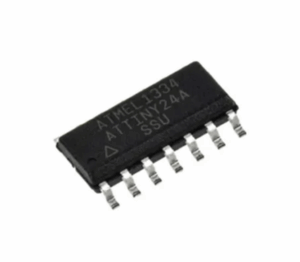
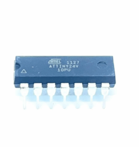
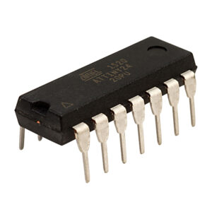
Extract Microcontroller ATtiny24V Flash describes a careful, authorized process: obtaining a readable binary image from a small, low-power MCU so organizations can recover lost program data, support aging products, or audit embedded software. The ATtiny24V is designed for compact, energy-sensitive applications — it combines modest on-chip flash and EEPROM with basic peripherals such as timers, ADC, and serial interfaces. These traits make it a common choice for battery-operated sensors, compact user interfaces, remote controls, simple home-automation modules, and low-cost instrumentation where minimal footprint and predictable timing are priorities.
When an ATtiny24V is embedded into a product, the flash usually contains more than control loops: calibration tables, communication routines, and proprietary program logic often live in that memory alongside device configuration in EEPROM. Over time, companies can lose the original source repositories or face corrupted updates in the field. In such cases, engineers must read out the MCU’s flash to recover a binary or hex file that becomes the starting point for rebuilding, restoring, or verifying device behavior. Because manufacturers often set the chip to a protected or locked state to prevent unauthorized cloning, the recovery task involves legal and technical boundaries that must be respected.
Working with a secured device is rarely straightforward. The ATtiny24V’s small package and simple debug features mean that standard interfaces may be intentionally disabled; a direct program dump is not always available by default. Even after a successful readout, the resulting file is a compiled archive — dense, optimized machine code without comments or symbols — which requires careful analysis to interpret. This reverse engineering step is essential when a client needs to replicate functionality, restore a corrupted unit, or validate that a device implements required safety controls. Importantly, such analysis focuses on recovering and preserving the firmware’s intent, not enabling unauthorized copying or distribution.
Extract Microcontroller ATtiny24V Flash content will become avilable after crack mcu attiny24v fuse bit and break protective avr chip attiny24v protection flash memory;
The AVR core combines a rich instruction set with 32 general purpose working registers. All the 32 registers are directly connected to the Arithmetic Logic Unit (ALU), allowing two independent registers to be accessed in one single instruction executed in one clock cycle.
The resulting architecture is more code efficient while achieving throughputs up to ten times faster than conventional CISC microcontrollers.
The ATtiny24/44/84 provides the following features: 2/4/8K byte of In-System Programmable Flash, 128/256/512 bytes EEPROM, 128/256/512 bytes SRAM, 12 general purpose I/O lines, 32 general purpose working registers, a 8-bit Timer/Counter with two PWM channels, a 16-bit timer/counter with two PWM channels, Internal and External Interrupts, a 8-channel 10-bit ADC, programmable gain stage (1x, 20x) for 12 differential ADC channel pairs, a programmable Watchdog Timer with internal Oscillator, internal calibrated oscillator, and three software selectable power saving modes.
The Idle mode stops the CPU while allowing the SRAM, Timer/Counter, ADC, Analog Comparator, and Interrupt system to continue functioning. The Power-down mode saves the register contents, disabling all chip functions until the next Interrupt or Hardware Reset.
The practical benefits to clients are clear and measurable. Recovering a verified firmware image can dramatically shorten repair cycles and reduce field downtime, because technicians can re-flash affected units or produce compatible replacements. For regulated products, having an archived program enables compliance checks and safety audits; auditors can inspect the recovered binary to confirm that certified control logic remains intact. In legacy scenarios, extracting the flash allows companies to lawfully replicate or restore discontinued products when source code or vendor support is unavailable, preserving critical infrastructure and business continuity.
Risks and constraints play a major role in deciding how to proceed. Physical board layouts, fragile package leads, and delicate EEPROM data make non-destructive handling essential; an unsuccessful attempt can irreversibly damage both chip and data. Legal and contractual permissions must be obtained before any work begins, and providers emphasize documented authorization and provenance to protect client IP and privacy. The goal is recovery, restoration, and long-term support — not piracy or clandestine copying.
The ADC Noise Reduction mode stops the CPU and all I/O modules except ADC, to minimize switching noise during ADC conversions. In Standby mode, the crystal/resonator Oscillator is running while the rest of the device is sleeping by extract attiny24 mcu source code. This allows very fast start-up combined with low power consumption.
The device is manufactured ng Atmel’s high density non-volatile memory technology. The On-chip ISP Flash allows the Program memory to be re-programmed In-System through an SPI serial interface, by a conventional non-volatile memory programmer or by an On-chip boot code running on the AVR core.
The ATtiny24/44/84 AVR is supported with a full suite of program and system development tools including: C Compilers, Macro Assemblers, Program Debugger/Simulators, In-Circuit Emulators, and Evaluation kits. Port B is a 4-bit bi-directional I/O port with internal pull-up resistors (selected for each bit).
The Port B output buffers have symmetrical drive characteristics with both high sink and source capability except PB3 which has the RESET capability. To use pin PB3 as an I/O pin, instead of RESET pin, program (‘0’) RSTDISBL fuse. As inputs, Port B pins that are externally pulled low will source current if the pull-up resistors are activated when Extract Microcontroller.
The Port B pins are tri-stated when a reset condition becomes active, even if the clock is not running. Port A is a 8-bit bi-directional I/O port with internal pull-up resistors (selected for each bit). The Port A output buffers have symmetrical drive characteristics with both high sink and source capability.
As inputs, Port A pins that are externally pulled low will source current if the pull-up resistors are activated. The Port A pins are tri-stated when a reset condition becomes active, even if the clock is not running.
In summary, Extract Microcontroller ATtiny24V Flash is a specialized, high-value capability that combines firmware recovery, ethical reverse engineering, and product lifecycle support. When performed responsibly, it returns a secured, previously inaccessible program archive into a usable form that helps clients maintain devices, validate safety, and extend the productive life of embedded systems.