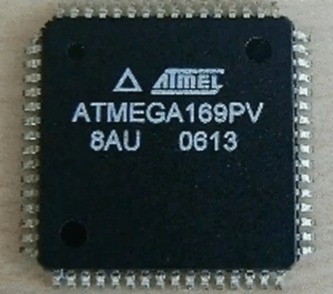
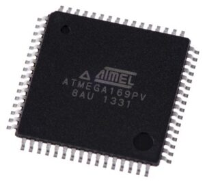
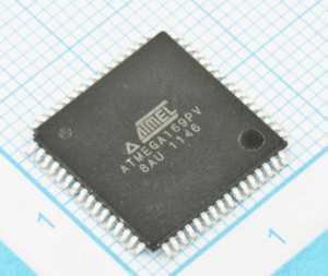
The process to extract Microcontroller ATmega169PV code is a sophisticated engineering task that deals with retrieving valuable firmware and binary data from a secured or locked integrated circuit. The ATmega169PV, a powerful 8-bit microcontroller from Microchip, is widely recognized for its energy efficiency, compact design, and stable performance. It is commonly used in industrial automation systems, electronic meters, smart home appliances, and various handheld consumer electronics where reliability and low power consumption are essential.
When a product enters the maintenance or redevelopment stage, access to its firmware becomes a key requirement. In many cases, the original source code or binary program stored in the MCU’s flash or EEPROM memory is no longer available. Here, reverse engineering techniques are applied to recover or restore the data. The task may involve reading, decoding, and dumping the binary archive from the protected memory. Because these chips are often encrypted, secured, or locked by design, engineers must overcome several technical barriers to ensure a successful program recovery without damaging the microcontroller.
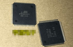
Extract Microcontroller ATmega169PV Code needs to crack mcu atmega169pv security fuse bit and recover locked heximal file from processor atmega169pv;
An EEPROM data corruption can be caused by two situations when the voltage is too low. First, a regular write sequence to the EEPROM requires a minimum voltage to operate correctly. Secondly, the CPU itself can execute instructions incorrectly, if the supply voltage is too low.
EEPROM data corruption can easily be avoided by following this design recommendation: Keep the AVR RESET active (low) during periods of insufficient power supply voltage. This can be done by enabling the internal Brown-out Detector (BOD). If the detection level of the internal BOD does not match the needed detection level, an external low VCC reset Protection circuit can be used.
The ATmega169PV features advanced security mechanisms, including fuse bits and lock bits that prevent unauthorized readout of flash or EEPROM data. This makes cloning, copying, or replicating the program highly challenging. The protection ensures intellectual property safety, but it also complicates legitimate efforts to repair, analyze, or rebuild existing hardware systems. Overcoming these barriers requires careful micro-level analysis, precise signal control, and knowledge of semiconductor behavior. While the methods to break, attack, or decode the chip are not revealed, the process demands high-end equipment, experience in data extraction, and an understanding of the microcontroller’s internal structure.
Why is this kind of work important? In many industrial and commercial cases, companies face the need to recover firmware from obsolete or discontinued devices. Re-engineering the original program allows them to extend the lifespan of their hardware, support product updates, or build compatible replacements. When a manufacturer no longer provides technical support or documentation, extracting and restoring the program archive from a secured MCU becomes the only way to sustain production or perform technical upgrades.
If a reset occurs while a write operation is in progress, the write operation will be completed provided that the power supply voltage is sufficient. The I/O space definition of the ATmega48/88/168 is shown in ”Register Summary” on page 342. All ATmega48/88/168 I/Os and peripherals are placed in the I/O space. All I/O locations may be accessed by the LD/LDS/LDD and ST/STS/STD instructions, transferring data between the 32 general purpose working registers and the I/O space.
I/O Registers within the address range 0x00 – 0x1F are directly bit-accessible using the SBI and CBI instructions. In these registers, the value of single bits can be checked by using the SBIS and SBIC instructions.
Refer to the instruction set section for more details. When using the I/O specific commands IN and OUT, the I/O addresses 0x00 – 0x3F must be used. When addressing I/O Registers as data space using LD and ST instructions, 0x20 must be added to these addresses. The ATmega48/88/168 is a complex microcontroller with more peripheral units than can be supported within the 64 location reserved in Opcode for the IN and OUT instructions.
For the Extended I/O space from 0x60 – 0xFF in SRAM, only the ST/STS/STD and LD/LDS/LDD instructions can be used. For compatibility with future devices, reserved bits should be written to zero if accessed. Reserved I/O memory addresses should never be written.
Some of the Status Flags are cleared by writing a logical one to them. Note that, unlike most other AVRs, the CBI and SBI instructions will only operate on the specified bit, and can therefore be used on registers containing such Status Flags. The CBI and SBI instructions work with registers 0x00 to 0x1F only.
The I/O and peripherals control registers are explained in later sections. The ATmega48/88/168 contains three General Purpose I/O Registers. These registers can be used for storing any information, and they are particularly useful for storing global variables and Status Flags. General Purpose I/O Registers within the address range 0x00 – 0x1F are directly bit-accessible using the SBI, CBI, SBIS, and SBIC instructions.
The EEPROM Read Enable Signal EERE is the read strobe to the EEPROM. When the correct address is set up in the EEAR Register, the EERE bit must be written to a logic one to trigger the EEPROM read. The EEPROM read access takes one instruction, and the requested data is available immediately. When the EEPROM is read, the CPU is halted for four cycles before the next instruction is executed.
The user should poll the EEPE bit before starting the read operation. If a write operation is in progress, it is neither possible to read the EEPROM, nor to change the EEAR Register. The calibrated Oscillator is used to time the EEPROM accesses. Table 6-2 lists the typical programming time for EEPROM access from the CPU.
The following code examples show one assembly and one C function for writing to the EEPROM. The examples assume that interrupts are controlled (e.g. by disabling interrupts globally) so that no interrupts will occur during execution of these functions. The examples also assume that no Flash Boot Loader is present in the software. If such code is present, the EEPROM write function must also wait for any ongoing SPM command to finish.
In the process of reverse engineering an ATmega169PV chip, engineers may face difficulties such as damaged packages, inaccessible debug interfaces, or data corruption during readout. Yet, with the right technology and expertise, it is possible to decrypt and reconstruct the essential firmware structure. Once the binary data has been recovered or duplicated, it can be analyzed, improved, or reused to create compatible versions of the original design.
Ultimately, the purpose of extracting the ATmega169PV firmware is not simply to copy or hack a chip, but to enable knowledge preservation, hardware continuity, and system redevelopment. It offers clients practical value—recovering lost intellectual property, maintaining production stability, and ensuring that vital embedded systems continue to operate for years to come.