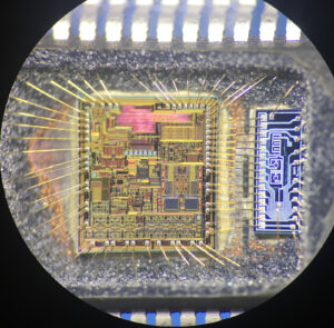
Extract MCU code of PIC16HV610 is a specialized technique designed for clients seeking to access firmware and program data from secured microcontrollers. This service employs advanced methods to crack, attack, decapsulate, hack, decrypt, decode, and reverse engineer the protected binary embedded in the chip. By leveraging our expertise, we recover, replicate, clone, extract, and dump data stored in the locked EEPROM and flash memory of the PIC16HV610 microcontroller.
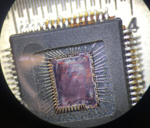
The PIC16HV610 is a robust microprocessor with built-in security features intended to safeguard its firmware and source code. Despite these measures, our process methodically overcomes these secured barriers by utilizing a precise combination of hardware and software techniques. Initially, the chip is decapsulated to expose the internal architecture, followed by a detailed attack on its encrypted memory. Specialized tools then extract the firmware and program files, which are stored as an archive of binary data. This allows us to replicate the chip’s complete program memory and even decode its source code for further analysis.
Our service is ideal for clients needing to recover critical data from protected devices, ensuring a reliable, efficient, and secure method to extract MCU code of PIC16HV610 while maintaining data integrity and compliance.
All peripherals and modules are addressable through I/O memory locations in the data memory space in the process of Extract MCU Code of PIC16HV610. All I/O memory locations can be accessed by the Load (LD/LDS/LDD) and Store (ST/STS/STD) instructions, transferring data between the 32 general purpose registers in the CPU and the I/O Memory.
The IN and OUT instructions can address I/O memory locations in the range 0x00 – 0x3F directly. I/O registers within the address range 0x00 – 0x1F are directly bit-accessible using the SBI and CBI instructions.
The value of single bits can be checked by using the SBIS and SBIC instructions on these registers
The PIC16HV610 devices has internal EEPROM memory for non-volatile data storage. It is addressable either in a separate data space or it can be memory mapped into the normal data memory space. The EEPROM memory supports both byte and page access.
- Supports SRAM up to
– 512K Bytes using 2-port EBI
– 16M Bytes using 3-port EBI
Supports SDRAM up to
– 128M bit using 3-port EBI
Four software configurable Chip Selects
Software configurable Wait State insertion
Clocked from the Peripheral 2x Clock at up to two times the CPU clock speed
The External Bus Interface (EBI) is the interface for connecting external peripheral and memory to the data memory space. The PIC16HV610 has 3 ports that can be used for the EBI. It can interface external SRAM, SDRAM, and/or peripherals such as LCD displays and other memory mapped devices and this mechanism will facilitate the process of Program From Encrypted MCU PIC16LF873 copying.
The address space, and the number of pins used, for the external memory is selectable from 256 bytes (8-bit) and up to 16M bytes (24-bit).
Various multiplexing modes for address and data lines can be selected for optimal use of pins when more or less pins is available for the EBI. Each of the four chip selects has seperate configuration, and can be configured for SRAM, SRAM Low Pin Count (LPC) or SDRAM. The data memory address space associated for each chip select is decided by a configurable base address and address size for each chip select.
For SDRAM both 4-bit SDRAM is supported, and SDRAM configurations such as CAS Latency and Refresh rate is configurable in software obtained from Microchip Microprocessor PIC16LF874 Heximal Extraction. The EBI is clocked from the Peripheral 2x Clock, running up to two times faster than the CPU and supporting speeds of up to 64 MHz. The Calibration Row is a seperate memory section for factory programmed data when Extract MCU Code of PIC16HV610.
It contains calibration data for functions such as oscillators, device ID, and a factory programmed serial number that is unique for each device. The device ID for the available PIC16HV610 devices is shown in Table 7-1 on page 13. Some of the calibration values will be automatically loaded to the corresponding module or peripheral unit during reset.
The Calibration Row can not be written or erased. It can be read from application software and external programming by MCU Cracking.