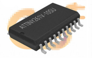
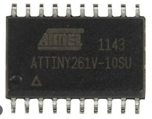
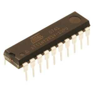
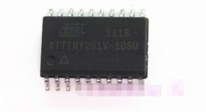
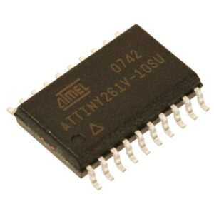
The need to extract MCU ATtiny261V code is growing rapidly as manufacturers, engineers, and product owners rely heavily on compact embedded solutions for long-term system performance. The ATtiny261V is a low-power yet capable 8-bit microcontroller, equipped with 2 KB of flash, internal EEPROM, a flexible timer system, an advanced PWM generator, and multiple analog and digital peripherals. Its wide operating voltage range and efficient power consumption allow it to be deployed in battery-powered instruments, portable controllers, home automation devices, industrial sensing modules, LED driver boards, and compact motor-control systems.
In many real-world situations, the only remaining copy of the original firmware, binary, or source code resides within the microcontroller itself. Documentation may be lost, suppliers may discontinue support, or engineers may need to recover the operational logic of a legacy device. In these circumstances, organizations seek to open, extract, or restore the flash, EEPROM, and configuration data stored inside the ATtiny261V. However, gaining access to this information is not a trivial process. The chip typically employs secured, protected, encrypted, or locked fuse settings that prevent unauthorized copying or duplication.
Extract MCU ATtiny261V Code from its locked memory, break microcontroller attiny261 tamper resistance system and readout the embedded firmware from MCU;
The AVR core combines a rich instruction set with 32 general purpose working registers. All the 32 registers are directly connected to the Arithmetic Logic Unit (ALU), allowing two independent registers to be accessed in one single instruction executed in one clock cycle.
The resulting architecture is more code efficient while achieving throughputs up to ten times faster than conventional CISC microcontrollers.
The ATtiny261/461/861 provides the following features: 2/4/8K byte of In-System Programmable Flash, 128/256/512 bytes EEPROM, 128/256/512 bytes SRAM, 6 general purpose I/O lines, 32 general purpose working registers, one 8-bit Timer/Counter with compare modes, one 8-bit high speed Timer/Counter, Universal Serial Interface, Internal and External Interrupts, a 4-channel, 10-bit ADC, a programmable Watchdog Timer with internal Oscillator, and three software selectable power saving modes.
Overcoming such protections requires specialized reverse-engineering capabilities. Although the process may be described informally as a hack, it is, in fact, a controlled, technical operation involving analysis of the microcontroller architecture and careful manipulation of the chip’s internal memory domains. The objective is to generate a clean program dump, complete heximal archive, or fully readable program file without damaging the device or introducing inconsistencies in the extracted program.
The difficulties arise from multiple embedded safeguards: locked readout fuses, encrypted memory blocks, and structured protection schemes that resist straightforward access. Each ATtiny261V must be handled with precision to ensure that the archive of program logic recovered from the MCU is accurate and complete. While the methodologies involved remain proprietary, the expertise applied ensures reliability and repeatability.
The Idle mode stops the CPU while allowing the SRAM, Timer/Counter, ADC, Analog Comparator, and Interrupt system to continue functioning.
The Power-down mode saves the register contents, disabling all chip functions until the next Interrupt or Hardware Reset. The ADC Noise Reduction mode stops the CPU and all I/O modules except ADC, to minimize switching noise during ADC conversions.
The device is manufactured using Atmel’s high density non-volatile memory technology. The On-chip ISP Flash allows the Program memory to be re-programmed In-System through an SPI serial interface, by a conventional non-volatile memory programmer or by an On-chip boot code running on the AVR core.
The ATtiny261/461/861 AVR is supported with a full suite of program and system development tools including: C Compilers, Macro Assemblers, Program Debugger/Simulators, In-Circuit Emulators, and Evaluation kits.
Port A is an 8-bit bi-directional I/O port with internal pull-up resistors (selected for each bit). The Port A output buffers have symmetrical drive characteristics with both high sink and source capability.
As inputs, Port A pins that are externally pulled low will source current if the pull-up resistors are activated. The Port A pins are tri-stated when a reset condition becomes active, even if the clock is not running.
Port B is an 8-bit bi-directional I/O port with internal pull-up resistors (selected for each bit). The Port B output buffers have symmetrical drive characteristics with both high sink and source capability.
As inputs, Port B pins that are externally pulled low will source current if the pull-up resistors are activated. The Port B pins are tri-stated when a reset condition becomes active, even if the clock is not running.
- For compatibility with future devices, reserved bits should be written to zero if accessed. Reserved I/O memory addresses should never be written.
- I/O Registers within the address range 0x00 – 0x1F are directly bit-accessible using the SBI and CBI instructions. In these registers, the value of single bits can be checked by using the SBIS and SBIC instructions after Extract MCU.
- Some of the Status Flags are cleared by writing a logical one to them. Note that, unlike most other AVRs, the CBI and SBI instructions will only operation the specified bit, and can therefore be used on registers containing such Status Flags. The CBI and SBI instructions work with registers 0x00 to 0x1F only.
Extracting the embedded program offers significant value to clients. It allows companies to continue operating or refurbishing legacy devices, reproduce discontinued control boards, or redesign products without rebuilding the entire firmware from scratch. It supports quality validation, functional analysis, system upgrading, and compatibility redevelopment. Ultimately, extracting ATtiny261V code provides a practical and cost-efficient path to preserving intellectual assets, extending product lifecycles, and enabling sustainable technology migration.
Through advanced reverse engineering and precision extraction workflows, we transform protected microcontroller memory into accessible, actionable engineering knowledge—supporting long-term resilience and uninterrupted business operations.