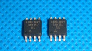
Extract MCU ATTINY15L Code from secured microcontroller attiny15L flash memory, the status of microprocessor attiny15l will be reset from locked to unlocked;
The ALU supports arithmetic and logic functions between registers or between a constant and a register. Single-register operations are also executed in the ALU. Figure 2 shows the ATtiny15L AVR RISC microcontroller architecture. The AVR uses a Harvard architecture concept with separate memories and buses for program and data memories.
The program memory is accessed with a two-stage pipeline. While one instruction is being executed, the next instruction is pre-fetched from the program memory. This concept enables instructions to be executed in every clock cycle. The program memory is In-System Programmable Flash memory.
With the relative jump and relative call instructions, the whole address space is directly accessed. All AVR instructions have a single 16-bit word format, meaning that every program memory address contains a single 16-bit instruction by extract ic attiny15 software. During interrupts and subroutine calls, the return address program counter (PC) is stored on the stack. The stack is a 3-level-deep hardware stack dedicated for subroutines and interrupts.
The I/O memory space contains 64 addresses for CPU peripheral functions as Control Registers, Timer/Counters and other I/O functions. The memory spaces in the AVR architecture are all linear and regular memory maps. A flexible interrupt module has its control registers in the I/O space with an additional global interrupt enable bit in the status register.
All the different interrupts have a separate interrupt vector in the interrupt vector table at the beginning of the program memory. The different interrupts have priority in accordance with their interrupt vector position. The lower the interrupt vector address, the higher the priority.
All the register operating instructions in the instruction set have direct- and single-cycle access to all registers. The only exception is the five constant arithmetic and logic instructions SBCI, SUBI, CPI, ANDI, and ORI between a constant and a register and the LDI instruction for load-immediate constant data.
These instructions apply to the second half of the registers in the register file – R16..R31. The general SBC, SUB, CP, AND, OR, and all other operations between two registers or on a single-register apply to the entire register file. Registers 30 and 31 form a 16-bit pointer (the Z-pointer) which is used for indirect Flash memory and register file access. When the Register file is accessed, the contents of R31 is discarded by the CPU.
The high-performance AVR ALU operates in direct connection with all the 32 general purpose working registers. Within a single clock cycle, ALU operations between registers in the register file are executed. The ALU operations are divided into three main categories – arithmetic, logic and bit-functions. Some microcontrollers in the AVR product family feature a hardware multiplier in the arithmetic part of the ALU.